SBAS649B June   2021  – June 2022 DAC12DL3200

PRODUCTION DATA  

  1. Features
  2. Applications
  3. Description
  4. Revision History
  5. Pin Configuration and Functions
  6. Specifications
    1. 6.1  Absolute Maximum Ratings
    2. 6.2  ESD Ratings
    3. 6.3  Recommended Operating Conditions
    4. 6.4  Thermal Information
    5. 6.5  Electrical Characteristics - DC Specifications
    6. 6.6  Electrical Characteristics - Power Consumption
    7. 6.7  Electrical Characteristics - AC Specifications
    8. 6.8  Timing Requirements
    9. 6.9  Switching Characteristics
    10. 6.10 Typical Characteristics
  7. Detailed Description
    1. 7.1 Overview
    2. 7.2 Functional Block Diagram
    3. 7.3 Feature Description
      1. 7.3.1 DAC Output Modes
        1. 7.3.1.1 NRZ Mode
        2. 7.3.1.2 RTZ Mode
        3. 7.3.1.3 RF Mode
        4. 7.3.1.4 2xRF Mode
      2. 7.3.2 DAC Output Interface
        1. 7.3.2.1 DAC Output Structure
        2. 7.3.2.2 Full-scale Current Adjustment
        3. 7.3.2.3 Example Analog Output Interfaces
      3. 7.3.3 LVDS Interface
        1. 7.3.3.1 MODE0: Two LVDS banks per channel
        2. 7.3.3.2 MODE1: One LVDS bank per channel
        3. 7.3.3.3 MODE2: Four LVDS banks, single channel mode
        4. 7.3.3.4 LVDS Interface Input Strobe
        5. 7.3.3.5 FIFO Operation
          1. 7.3.3.5.1 Using FIFO Delay Readback Values
          2. 7.3.3.5.2 FIFO Delay Handling
          3. 7.3.3.5.3 FIFO Delay and NCO Operation
          4. 7.3.3.5.4 FIFO Over/Under Flow Alarming
      4. 7.3.4 Multi-Device Synchronization (SYSREF+/-)
        1. 7.3.4.1 DACCLK Domain Synchronization
        2. 7.3.4.2 SYSREF Position Detector and Sampling Position Selection (SYSREF Windowing)
      5. 7.3.5 Alarms
    4. 7.4 Device Functional Modes
      1. 7.4.1 Direct Digital Synthesis (DDS) Mode
        1. 7.4.1.1 NCO Gain Scaling
        2. 7.4.1.2 NCO Phase Continuous Operation
        3. 7.4.1.3 Trigger Clock
    5. 7.5 Programming
      1. 7.5.1 Using the Serial Interface
        1. 7.5.1.1 SCS
        2. 7.5.1.2 SCLK
        3. 7.5.1.3 SDI
        4. 7.5.1.4 SDO
        5. 7.5.1.5 Serial Interface Operation
        6. 7.5.1.6 Streaming Mode
      2. 7.5.2 SPI Register Map
  8. Application and Implementation
    1. 8.1 Application Information
      1. 8.1.1 Startup Procedure with LVDS Input
      2. 8.1.2 Startup Procedure With NCO Operation
      3. 8.1.3 Interface Test Pattern and Timing Verification
    2. 8.2 Typical Application
      1. 8.2.1 Design Requirements
      2. 8.2.2 Detailed Design Procedure
      3. 8.2.3 Application Curves
    3. 8.3 Power Supply Recommendations
      1. 8.3.1 Power Up and Down Sequence
    4. 8.4 Layout
      1. 8.4.1 Layout Guidelines
      2. 8.4.2 Layout Example
  9. Device and Documentation Support
    1. 9.1 Receiving Notification of Documentation Updates
    2. 9.2 Support Resources
    3. 9.3 Trademarks
    4. 9.4 Electrostatic Discharge Caution
    5. 9.5 Glossary
  10. 10Mechanical, Packaging, and Orderable Information

Package Options

Mechanical Data (Package|Pins)
Thermal pad, mechanical data (Package|Pins)
Orderable Information

MODE1: One LVDS bank per channel

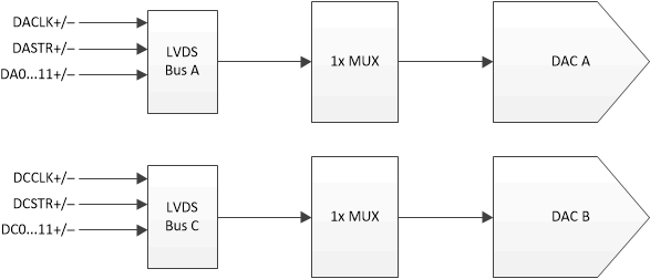
MODE1 uses one 12-bit LVDS data bus per channel. One dual-data rate (DDR) clock is used for each 12-bit LVDS data bus resulting in two total data clocks. This mode allows one fourth of the maximum sampling rate of the DAC. Table 7-5 shows the LVDS bus, data clock and strobe assignments for each channel. Figure 7-15 shows the block diagram for this mode for further understanding, including the signal assignments.

Table 7-5 MODE1 LVDS Bus, Data Clock and Strobe Signal Assignments
DAC CHANNELLVDS BUSESDATA CLOCKSSTROBE USED
AADACLKDASTR
BCDCCLKDCSTR
GUID-2AECB6F5-FAA4-4DFE-8654-BD5D17AB1E93-low.gifFigure 7-15 MODE1 Block Diagram

Figure 7-16 shows the functional timing diagram for MODE1. Two 12-bit buses are used, with bus A for DAC channel A data and bus C for DAC channel B data. There is no strict timing skew requirement between LVDS buses (e.g. A to C) as long as the internal FIFOs maintain sufficient offset between read and write pointers.

Figure 7-16 MODE1 Functional Timing Diagram