SLAS959D August 2013 – February 2018 DAC3151 , DAC3161 , DAC3171
PRODUCTION DATA.
- 1 Features
- 2 Applications
- 3 Description
- 4 Revision History
- 5 Pin Configuration and Functions
-
6 Specifications
- 6.1 Absolute Maximum Ratings
- 6.2 ESD Ratings
- 6.3 Recommended Operating Conditions
- 6.4 Thermal Information
- 6.5 Electrical Characteristics: DC Specifications
- 6.6 Electrical Characteristics: AC Specifications
- 6.7 Electrical Characteristics: Digital Specifications
- 6.8 Timing Requirements
- 6.9 Typical Characteristics
-
7 Detailed Description
- 7.1 Overview
- 7.2 Functional Block Diagrams
- 7.3 Feature Description
- 7.4 Device Functional Modes
- 7.5 Programming
- 7.6
Register Map
- 7.6.1 Register Name: config0 – Address: 0x00, Default: 0x4FC
- 7.6.2 Register Name: config1 – Address: 0x01, Default: 0x600E
- 7.6.3 Register Name: config2 – Address: 0x02, Default: 0x3FFF
- 7.6.4 Register Name: config3 – Address: 0x03, Default: 0x0000
- 7.6.5 Register Name: config4 – Address: 0x04, Default: 0x0000
- 7.6.6 Register Name: config5 – Address: 0x05, Default: 0x0000
- 7.6.7 Register Name: config6 – Address: 0x06, Default: 0x0010(DAC3171); 0x0094(DAC3161); 0x0098(DAC3151)
- 7.6.8 Register Name: config7 – Address: 0x07, Default: 0xFFFF
- 7.6.9 Register Name: config8 – Address: 0x08, Default: 0x6000
- 7.6.10 Register Name: config9 – Address: 0x09, Default: 0x8000
- 7.6.11 Register name: config10 – Address: 0x0A, Default: 0xF080
- 7.6.12 Register Name: config11 – Address: 0x0B, Default: 0x1111
- 7.6.13 Register Name: config12 – Address: 0x0C, Default: 0x3A7A
- 7.6.14 Register Name: config13 – Address: 0x0D, Default: 0x36B6
- 7.6.15 Register Name: config14 – Address: 0x0E, Default: 0x2AEA
- 7.6.16 Register name: config15 – Address: 0x0F, Default: 0x0545
- 7.6.17 Register Name: config16 – Address: 0x10, Default: 0x0585
- 7.6.18 Register Name: config17 – Address: 0x11, Default: 0x0949
- 7.6.19 Register Name: config18 – Address: 0x12, Default: 0x1515
- 7.6.20 Register Name: config19 – Address: 0x13, Default: 0x3ABA
- 7.6.21 Register Name: config20– Address: 0x14, Default: 0x0000
- 7.6.22 Register Name: config21– Address: 0x15, Default: 0xFFFF
- 7.6.23 Register Name: config22– Address: 0x16, Default: 0x0000
- 7.6.24 Register Name: config23– Address: 0x17, Default: 0x0000
- 7.6.25 Register Name: config24– Address: 0x18, Default: 0x0000
- 7.6.26 Register Name: config25– Address: 0x19, Default: 0x0000
- 7.6.27 Register Name: config127– Address: 0x7F, Default: 0x0045
- 8 Application and Implementation
- 9 Power Supply Recommendations
- 10Layout
- 11Device and Documentation Support
- 12Mechanical, Packaging, and Orderable Information
Package Options
Mechanical Data (Package|Pins)
- RGC|64
Thermal pad, mechanical data (Package|Pins)
- RGC|64
Orderable Information
8.2.2 Detailed Design Procedure
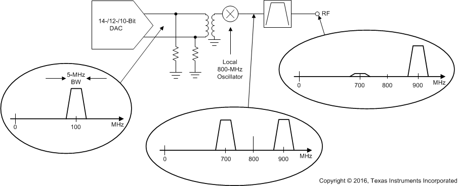
The data pattern file that represents the desired 5-MHz, single-carrier WCDMA signal is created with a pattern generation is clocked into the DAC31x1 by an FPGA as shown in the Figure 72. We choose to generate the data pattern file with the 5-MHz WCDMA signal centered at an intermediate frequency of 100 MHz and use a local oscillator of 800 MHz to upconvert the modulated signal to 900 MHz. The real mixer will create an image of the desired signal centered about 700 MHz, and there will also be local oscillator (LO) feedthrough observed at 800 MHz. A band-pass filter that follows the mixer is needed to remove the lower image of the signal and the local oscillator feedthrough, as shown in Figure 73.
 Figure 73. Signal Spectrum in a Real IF Transmitter
The choice of the intermediate frequency has an impact on the design of the 900-MHz band-pass filter. The band-pass filter is to pass the WCDMA signal image that is centered at 900 MHz, but provide significant attenuation of the local oscillator feedthrough and the signal image. The distance between the signal and the image is equal to twice the intermediate frequency. If the intermediate frequency is too low, the image gets too close to the signal, then a higher order band pass filter with steep roll-off is required. If the intermediate frequency is too high, the image would be further away from the signal, but the signal would be too far out towards the end of the Nyquist zone, and the SinX/X distortion would become an issue. Centering the DAC output signal at an intermediate frequency of 100 MHz is a good and balanced choice in this example, making the design of the band-pass filter reasonably easy.
The DAC31x1 does not have an interpolation option, so the data rate for the sample data will be the same rate as the sample rate to the DAC31x1. In this case, we choose a sample rate of 500 MSPS, the maximum sample rate for this device.