SLASEH3A October 2020 – May 2021 DAC61402 , DAC81402
PRODUCTION DATA
- 1 Features
- 2 Applications
- 3 Description
- 4 Revision History
- 5 Device Comparison Table
- 6 Pin Configuration and Functions
-
7 Specifications
- 7.1 Absolute Maximum Ratings
- 7.2 ESD Ratings
- 7.3 Recommended Operating Conditions
- 7.4 Thermal Information
- 7.5 Electrical Characteristics
- 7.6 Timing Requirements: Write, IOVDD: 1.7 V to 2.7 V
- 7.7 Timing Requirements: Write, IOVDD: 2.7 V to 5.5 V
- 7.8 Timing Requirements: Read and Daisy Chain, FSDO = 0, IOVDD: 1.7 V to 2.7 V
- 7.9 Timing Requirements: Read and Daisy Chain, FSDO = 1, IOVDD: 1.7 V to 2.7 V
- 7.10 Timing Requirements: Read and Daisy Chain, FSDO = 0, IOVDD: 2.7 V to 5.5 V
- 7.11 Timing Requirements: Read and Daisy Chain, FSDO = 1, IOVDD: 2.7 V to 5.5 V
- 7.12 Timing Diagrams
- 7.13 Typical Characteristics
-
8 Detailed Description
- 8.1 Overview
- 8.2 Functional Block Diagram
- 8.3 Feature Description
- 8.4 Device Functional Modes
- 8.5 Programming
- 8.6
Register Map
- 8.6.1 NOP Register (address = 00h) [reset = 0000h]
- 8.6.2 DEVICEID Register (address = 01h) [reset = 0A70h or 0930h]
- 8.6.3 STATUS Register (address = 02h) [reset = 0000h]
- 8.6.4 SPICONFIG Register (address = 03h) [reset = 0AA4h]
- 8.6.5 GENCONFIG Register (address = 04h) [reset = 4000h]
- 8.6.6 BRDCONFIG Register (address = 05h) [reset = 000Fh]
- 8.6.7 SYNCCONFIG Register (address = 06h) [reset = 0000h]
- 8.6.8 DACPWDWN Register (address = 09h) [reset = FFFFh]
- 8.6.9 DACRANGE Register (address = 0Ah) [reset = 0000h]
- 8.6.10 TRIGGER Register (address = 0Eh) [reset = 0000h]
- 8.6.11 BRDCAST Register (address = 0Fh) [reset = 0000h]
- 8.6.12 DACn Register (address = 11h to 12h) [reset = 0000h]
- 9 Application and Implementation
- 10Power Supply Recommendations
- 11Layout
- 12Device and Documentation Support
- 13Mechanical, Packaging, and Orderable Information
Package Options
Mechanical Data (Package|Pins)
- RHB|32
Thermal pad, mechanical data (Package|Pins)
- RHB|32
Orderable Information
8.5.2 Daisy-Chain Operation
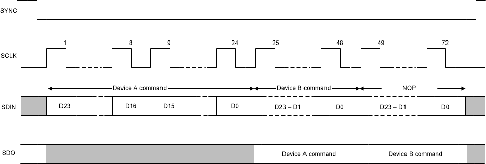
For systems that contain several devices, the SDO pin can be used to daisy-chain the devices together. Daisy-chain operation is useful in reducing the number of serial interface lines.The SDO pin must be enabled by setting the SDO-EN bit before initiating daisy-chain operation.
The first falling edge on the SYNC pin starts the operation cycle (see Figure 8-4). If more than 24 clock pulses are applied while the SYNC pin is kept low, the data ripple out of the shift register and are clocked out on the SDO pin, either on the falling edge or rising edge of SCLK according to the FSDO bit. By connecting the SDO output of the first device to the SDIN input of the next device in the chain, a multiple-device interface is constructed.
Each device in the daisy-chain system requires 24 clock pulses. As a result the total number of clock cycles must be equal to 24 × N, where N is the total number of devices in the daisy chain. When the serial transfer to all devices is complete, the SYNC signal is taken high. This action transfers the data from the SPI shift registers to the internal register of each device in the daisy chain, and prevents any further data from being clocked into the input shift register.
 Figure 8-4 Serial Interface Daisy-Chain Write
Cycle