SLASEH3A October 2020 – May 2021 DAC61402 , DAC81402
PRODUCTION DATA
- 1 Features
- 2 Applications
- 3 Description
- 4 Revision History
- 5 Device Comparison Table
- 6 Pin Configuration and Functions
-
7 Specifications
- 7.1 Absolute Maximum Ratings
- 7.2 ESD Ratings
- 7.3 Recommended Operating Conditions
- 7.4 Thermal Information
- 7.5 Electrical Characteristics
- 7.6 Timing Requirements: Write, IOVDD: 1.7 V to 2.7 V
- 7.7 Timing Requirements: Write, IOVDD: 2.7 V to 5.5 V
- 7.8 Timing Requirements: Read and Daisy Chain, FSDO = 0, IOVDD: 1.7 V to 2.7 V
- 7.9 Timing Requirements: Read and Daisy Chain, FSDO = 1, IOVDD: 1.7 V to 2.7 V
- 7.10 Timing Requirements: Read and Daisy Chain, FSDO = 0, IOVDD: 2.7 V to 5.5 V
- 7.11 Timing Requirements: Read and Daisy Chain, FSDO = 1, IOVDD: 2.7 V to 5.5 V
- 7.12 Timing Diagrams
- 7.13 Typical Characteristics
-
8 Detailed Description
- 8.1 Overview
- 8.2 Functional Block Diagram
- 8.3 Feature Description
- 8.4 Device Functional Modes
- 8.5 Programming
- 8.6
Register Map
- 8.6.1 NOP Register (address = 00h) [reset = 0000h]
- 8.6.2 DEVICEID Register (address = 01h) [reset = 0A70h or 0930h]
- 8.6.3 STATUS Register (address = 02h) [reset = 0000h]
- 8.6.4 SPICONFIG Register (address = 03h) [reset = 0AA4h]
- 8.6.5 GENCONFIG Register (address = 04h) [reset = 4000h]
- 8.6.6 BRDCONFIG Register (address = 05h) [reset = 000Fh]
- 8.6.7 SYNCCONFIG Register (address = 06h) [reset = 0000h]
- 8.6.8 DACPWDWN Register (address = 09h) [reset = FFFFh]
- 8.6.9 DACRANGE Register (address = 0Ah) [reset = 0000h]
- 8.6.10 TRIGGER Register (address = 0Eh) [reset = 0000h]
- 8.6.11 BRDCAST Register (address = 0Fh) [reset = 0000h]
- 8.6.12 DACn Register (address = 11h to 12h) [reset = 0000h]
- 9 Application and Implementation
- 10Power Supply Recommendations
- 11Layout
- 12Device and Documentation Support
- 13Mechanical, Packaging, and Orderable Information
Package Options
Mechanical Data (Package|Pins)
- RHB|32
Thermal pad, mechanical data (Package|Pins)
- RHB|32
Orderable Information
8.3.2 Programmable-Gain Output Buffer
The voltage output stage as conceptualized in Figure 8-3 provides the voltage output according to the DAC code and the output range setting.
 Figure 8-3 Voltage Output Buffer
For unipolar output mode, the output range can be programmed as:
- 0 V to 5 V
- 0 V to 10 V
- 0 V to 20 V
- 0 V to 40 V
For bipolar output mode, the output reange can be programmed as:
- ±5 V
- ±10 V
- ±20 V
In addition, 20% overrange is available on all ranges except for 0 V to 40 V and ±20 V.
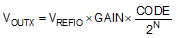
The input data are written to the individual DAC data registers in straight-binary format for all output ranges. The output voltage (VOUTX) can be expressed as Equation 1 and Equation 2.
For unipolar output mode
For bipolar output mode
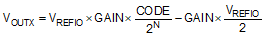
- CODE is the decimal equivalent of the binary code loaded to the DAC data register.
- N is the DAC resolution in bits.
- VREFIO is the reference voltage (internal or external).
- GAIN is the gain factor assigned to each output voltage output range as shown in Table 8-1.
| MODE | VOLTAGE OUTPUT RANGE | GAIN |
|---|---|---|
| Unipolar | 5 V | 2.0 |
| 6 V (20% overrange) | 2.4 | |
| 10 V | 4.0 | |
| 12 V (20% overrange) | 4.8 | |
| 20 V | 8.0 | |
| 24 V (20% overrange) | 9.6 | |
| 40 V | 16.0 | |
| Bipolar | ±5 V | 4.0 |
| ±6 V (20% overrange) | 4.8 | |
| ±10 V | 8.0 | |
| ±12 V (20% overrange) | 9.6 | |
| ±20 V | 16.0 |
The output amplifiers can drive up to ±15 mA with 1.5-V supply headroom while maintaining the specified TUE specification for the device. The output stage has short-circuit current protection that limits the output current to 40 mA. The device is able to drive capacitive loads up to 1 µF. For loads greater than 2 nF, an external compensation capacitor must be connected between the CCOMPx and OUTx pins to keep the output voltage stable, but at the expense of reduced bandwidth and increased settling time.