SBASAK3A September 2022 – November 2022 DAC82001
PRODUCTION DATA
- 1 Features
- 2 Applications
- 3 Description
- 4 Revision History
- 5 Pin Configuration and Functions
- 6 Specifications
- 7 Detailed Description
- 8 Application and Implementation
- 9 Device and Documentation Support
- 10Mechanical, Packaging, and Orderable Information
Package Options
Mechanical Data (Package|Pins)
- DRX|10
Thermal pad, mechanical data (Package|Pins)
Orderable Information
7.3.2 Power-On Reset (POR)
The DAC82001 device includes a power-on reset function that controls the output voltage at power up. After the VDD supply has been established, a POR event is issued. The POR causes all registers to initialize to default values, and communication with the device is valid only after a 250-µs, power-on-reset delay. The default value for all DACs is zero code if RSTSEL = AGND, and midscale code if RSTSEL = VDD. The DAC channel remains at the power-up voltage until a valid command is written to the channel.
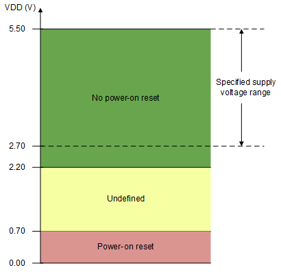
When the device powers up, a POR circuit sets the device to the default mode. Figure 7-2 shows that the POR circuit requires specific VDD levels to make sure that the internal capacitors discharge and reset the device at power up. To make sure that a POR occurs, VDD must be less than 0.7 V for at least 1 ms. When VDD drops to less than 2.2 V but remains greater than 0.7 V (shown as the undefined region in Figure 7-2), the device may or may not reset under all specified temperature and power-supply conditions; in this case, initiate a POR. When VDD remains greater than 2.2 V, a POR does not occur.
 Figure 7-2 Threshold Levels for the
VDD POR Circuit