SBAS940 December 2018 DAC8742H
PRODUCTION DATA.
- 1 Features
- 2 Applications
- 3 Description
- 4 Revision History
- 5 Pin Configuration and Functions
- 6 Specifications
-
7 Detailed Description
- 7.1 Overview
- 7.2 Functional Block Diagram
- 7.3
Feature Description
- 7.3.1 HART Modulator
- 7.3.2 HART Demodulator
- 7.3.3 FOUNDATION FIELDBUS / PROFIBUS PA Manchester Encoder
- 7.3.4 FOUNDATION FIELDBUS / PROFIBUS PA Manchester Decoder
- 7.3.5 Internal Reference
- 7.3.6 Clock Configuration
- 7.3.7 Reset and Power-Down
- 7.3.8 Full-Duplex Mode
- 7.3.9 I/O Selection
- 7.3.10 Jabber Inhibitor
- 7.4 Device Functional Modes
- 7.5
Register Maps
- 7.5.1 CONTROL Register (Offset = 2h) [reset = 0x8042]
- 7.5.2 RESET Register (Offset = 7h) [reset = 0x0000]
- 7.5.3 MODEM_STATUS Register (Offset = 20h) [reset = 0x0000]
- 7.5.4 MODEM_IRQ_MASK Register (Offset = 21h) [reset = 0x0024]
- 7.5.5 MODEM_CONTROL Register (Offset = 22h) [reset = 0x0048]
- 7.5.6 FIFO_D2M Register (Offset = 23h) [reset = 0x0200]
- 7.5.7 FIFO_M2D Register (Offset = 24h) [reset = 0x0200]
- 7.5.8 FIFO_LEVEL_SET Register (Offset = 25h) [reset = 0x0000]
- 7.5.9 PAFF_JABBER Register (Offset = 27h) [reset = 0x0000]
- 8 Application and Implementation
- 9 Power Supply Recommendations
- 10Layout
- 11Device and Documentation Support
- 12Mechanical, Packaging, and Orderable Information
Package Options
Mechanical Data (Package|Pins)
- PBS|32
Thermal pad, mechanical data (Package|Pins)
- PBS|32
Orderable Information
8.2.2.1 DAC8742H HART Modem
In this design the DAC8742H internal reference and bandpass filter was chosen to optimize board area, consequently reducing form factor and cost. X7R, 10% accurate, bypass capacitances of 1-µF and 0.1-µF values were chosen for the reference and supplies, respectively.
The DAC8742H device interfaces with the MSP430FR5969, or other similar host controller, through a standard UART interface. The DAC8742H digital pins connected through this interface include UART_RTS, UART_OUT (TX), UART_IN (RX), and CD.
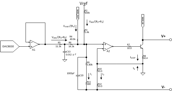
The remaining portion of the schematic includes other TI devices that aid in the realization of a highly accurate 4-mA to 20-mA, 2-wire transmitter. This combination of circuitry is ideally suited for remote signal conditioning of a wide variety of sensors and transducers, including thermocouples, RTDs, thermistors, and strain gauge bridges.
The two-wire transmitter is powered from an external DC power supply that is connected via the two BUS supply lines. The transmitter communicates by sourcing a 4-mA to 20-mA current through the connected bus, and back to the central host, which is typically a PLC analog input module. This expressed range of 4 mA to 20 mA is typically employed to adhere to industry standard, and ensures that the transmitter receives a minimum of 4 mA for correct powered operation.
 Figure 35. Simplified Schematic of the 2-Wire Current Loop