SBAS528D June   2013  – December 2021 DAC7760 , DAC8760

PRODUCTION DATA  

  1. Features
  2. Applications
  3. Description
  4. Revision History
  5. Device Comparison Table
  6. Pin Configuration and Functions
  7. Specifications
    1. 7.1  Absolute Maximum Ratings
    2. 7.2  ESD Ratings
    3. 7.3  Recommended Operating Conditions
    4. 7.4  Thermal Information
    5. 7.5  Electrical Characteristics
    6. 7.6  Electrical Characteristics: AC
    7. 7.7  Timing Requirements: Write Mode
    8. 7.8  Timing Requirements: Readback Mode
    9. 7.9  Timing Diagrams
    10. 7.10 Typical Characteristics
  8. Detailed Description
    1. 8.1 Overview
    2. 8.2 Functional Block Diagram
    3. 8.3 Feature Description
      1. 8.3.1  DAC Architecture
      2. 8.3.2  Voltage Output Stage
      3. 8.3.3  Current Output Stage
      4. 8.3.4  Internal Reference
      5. 8.3.5  Digital Power Supply
      6. 8.3.6  DAC Clear
      7. 8.3.7  Power-On Reset
      8. 8.3.8  Alarm Detection
      9. 8.3.9  Watchdog Timer
      10. 8.3.10 Frame Error Checking
      11. 8.3.11 User Calibration
      12. 8.3.12 Programmable Slew Rate
    4. 8.4 Device Functional Modes
      1. 8.4.1 Setting Voltage and Current Output Ranges
      2. 8.4.2 Boost Configuration for IOUT
      3. 8.4.3 Filtering the Current Output (only on the VQFN package)
      4. 8.4.4 HART Interface
        1. 8.4.4.1 For 4-mA to 20-mA Mode
        2. 8.4.4.2 For All Current Output Modes
    5. 8.5 Programming
      1. 8.5.1 Serial Peripheral Interface (SPI)
        1. 8.5.1.1 SPI Shift Register
        2. 8.5.1.2 Write Operation
        3. 8.5.1.3 Read Operation
        4. 8.5.1.4 Stand-Alone Operation
        5. 8.5.1.5 Multiple Devices on the Bus
    6. 8.6 Register Maps
      1. 8.6.1 DACx760 Command and Register Map
        1. 8.6.1.1 DACx760 Register Descriptions
          1. 8.6.1.1.1 Control Register
          2. 8.6.1.1.2 Configuration Register
          3. 8.6.1.1.3 DAC Registers
          4. 8.6.1.1.4 Reset Register
          5. 8.6.1.1.5 Status Register
  9. Application and Implementation
    1. 9.1 Application Information
      1. 9.1.1 Controlling the VOUT and IOUT Pins
        1. 9.1.1.1 VOUT and IOUT Pins are Independent Outputs, Never Simultaneously Enabled
        2. 9.1.1.2 VOUT and IOUT Pins are Independent Outputs, Simultaneously Enabled
        3. 9.1.1.3 VOUT and IOUT Pins are Tied Together, Never Simultaneously Enabled
      2. 9.1.2 Implementing HART in All Current Output Modes
        1. 9.1.2.1 Using CAP2 Pin on VQFN Package
        2. 9.1.2.2 Using the ISET-R Pin
      3. 9.1.3 Short-Circuit Current Limiting
    2. 9.2 Typical Application
      1. 9.2.1 Design Requirements
      2. 9.2.2 Detailed Design Procedure
      3. 9.2.3 Application Curves
  10. 10Power Supply Recommendations
  11. 11Layout
    1. 11.1 Layout Guidelines
      1. 11.1.1 Thermal Considerations
    2. 11.2 Layout Example
  12. 12Device and Documentation Support
    1. 12.1 Documentation Support
      1. 12.1.1 Related Documentation
    2. 12.2 Receiving Notification of Documentation Updates
    3. 12.3 Support Resources
    4. 12.4 Trademarks
    5. 12.5 Electrostatic Discharge Caution
    6. 12.6 Glossary
  13. 13Mechanical, Packaging, and Orderable Information

Package Options

Mechanical Data (Package|Pins)
Thermal pad, mechanical data (Package|Pins)
Orderable Information

Current Output Stage

The current output stage consists of a preconditioner and a current source as conceptualized in Figure 8-3. This stage provides a current output according to the DAC code. The output range can be programmed as 0 mA to
20 mA, 0 mA to 24 mA, or 4 mA to 20 mA. An external boost transistor can be used to reduce the power dissipation of the device. The maximum compliance voltage on pin IOUT equals (AVDD – 2 V). In single power-supply mode, the maximum AVDD is 36 V, and the maximum compliance voltage is 34 V. After power on, the IOUT pin is in a Hi-Z state.

GUID-CC1BB802-A785-4126-AD21-838854C636A9-low.gif Figure 8-3 Current Output

Resistor RSET (used to convert the DAC voltage to current) determines the stability of the output current over temperature. If desired, an external, low-drift, precision 15-kΩ resistor can be connected to the ISET-R pin and used instead of the internal RSET resistor.

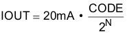
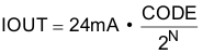
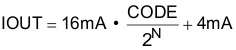
For a 5-V reference, the output can be expressed as shown in Equation 3 through Equation 5.

For a 0-mA to 20-mA output range:

Equation 3. GUID-0309C3F6-F490-41C3-88F8-8146CB5C9E99-low.gif

For a 0-mA to 24-mA output range:

Equation 4. GUID-12851227-DC77-4A29-8EC6-E8259D9C7335-low.gif

For a 4-mA to 20-mA output range:

Equation 5. GUID-C5FF1BA4-68DE-4218-8DFB-55E2DD64081D-low.gif

where

  • CODE is the decimal equivalent of the code loaded to the DAC.
  • N is the bits of resolution; 16 for DAC8760 and 12 for DAC7760.

The current-output range is normally set according to the value of the RANGE bits in the Control Register. When both the voltage and current outputs are enabled in dual-output mode, the range is set by the IOUT RANGE bits in the Configuration Register. See Section 8.4.1 for more details. For more details on controlling the current output when both the VOUT and IOUT pins are simultaneously enabled, see Section 9.1.1.