SBAS528D June 2013 – December 2021 DAC7760 , DAC8760
PRODUCTION DATA
- 1 Features
- 2 Applications
- 3 Description
- 4 Revision History
- 5 Device Comparison Table
- 6 Pin Configuration and Functions
- 7 Specifications
- 8 Detailed Description
- 9 Application and Implementation
- 10Power Supply Recommendations
- 11Layout
- 12Device and Documentation Support
- 13Mechanical, Packaging, and Orderable Information
Package Options
Mechanical Data (Package|Pins)
Thermal pad, mechanical data (Package|Pins)
Orderable Information
8.3.2 Voltage Output Stage
The voltage output stage as conceptualized in Figure 8-2 provides the voltage output according to the DAC code and the output range setting. The output range can be programmed as 0 V to 5 V or 0 V to 10 V for unipolar output mode, and ±5 V or ±10 V for bipolar output mode. In addition, an option is available to increase the output voltage range by 10%. The output current drive can be up to 10 mA. The output stage has short-circuit current protection that limits the output current to 30 mA. To maintain proper performance, a minimum 0.5-V power-supply headroom is required. The voltage output is able to drive a capacitive load up to 1 µF. For loads greater than 20 nF, to keep the output voltage stable at the expense of reduced bandwidth and increased settling time, connect an external compensation capacitor between CMP and VOUT. If an external compensation capacitor greater than 470 pF is used, connect an additional 100-pF capacitor from CMP to GND.
 Figure 8-2 Voltage Output
The +VSENSE pin is provided to enable sensing of the load by connecting to points electrically closer to the load. This configuration allows the internal output amplifier to make sure that the correct voltage is applied across the load, as long as headroom is available on the power supply. Ideally, this pin is used to correct for resistive drops on the system board and is connected to VOUT at the pins. In some cases, both VOUT and +VSENSE are brought out as pins and, through separate lines, connected remotely together at the load. In case the +VSENSE line is cut, use an optional 5-kΩ resistor between VOUT and +VSENSE to prevent the amplifier loop from breaking. The –VSENSE pin, on the other hand, is provided as a GND sense reference output from the internal VOUT amplifier. The output swing of the VOUT amplifier is relative to the voltage seen at this pin. The actual voltage difference between the –VSENSE pin and the device GND pins is not expected to be more than a few 100 µV. The internal resistor in Figure 8-2 between the device internal GND and the –VSENSE pin is typically 2 kΩ.
After power on, the power-on-reset circuit makes sure that all registers are at their default values. Therefore, the voltage output buffer is in a Hi-Z state; however, the +VSENSE pin connects to the amplifier inputs through an internal 60-kΩ feedback resistor (RFB in Figure 8-2). If the VOUT and +VSENSE pins are connected together, the VOUT pin is also connected to the same node through the feedback resistor. This node is protected by internal circuitry and settles to a value between GND and the reference input.
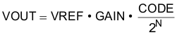
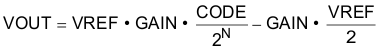
The output voltage (VOUT) can be expressed as Equation 1 and Equation 2.
For unipolar output mode:
For bipolar output mode:
where
- CODE is the decimal equivalent of the code loaded to the DAC
- N is the bits of resolution; 16 for DAC8760 and 12 for DAC7760
- VREF is the reference voltage; for internal reference, VREF = 5 V
- GAIN is automatically selected for a desired voltage output range as shown in Table 8-1
| VOLTAGE OUTPUT | GAIN |
|---|---|
| 0 V to 5 V | 1 |
| 0 V to 10 V | 2 |
| ±5 V | 2 |
| ±10 V | 4 |
The voltage range is set according to the value of the RANGE bits and the OVR bit in the Control Register. The OVR bit makes the gain value in Table 8-1 increase by 10%, thereby increasing the voltage output range, as shown in Table 8-8 (see Section 8.4.1 for more details).