SBAS438C May   2008  – November 2019 DAC9881

PRODUCTION DATA.  

  1. Features
  2. Applications
  3. Description
    1.     Device Images
      1.      Block Diagram
  4. Revision History
  5. Pin Configuration and Functions
    1.     Pin Functions
  6. Specifications
    1. 6.1  Absolute Maximum Ratings
    2. 6.2  ESD Ratings
    3. 6.3  Recommended Operating Conditions
    4. 6.4  Thermal Information
    5. 6.5  Electrical Characteristics: AVDD = 5 V
    6. 6.6  Electrical Characteristics: AVDD = 2.7 V
    7. 6.7  Timing Requirements—Standalone Operation Without SDO
    8. 6.8  Timing Requirements—Standalone Operation With SDO and Daisy-Chain Mode
    9. 6.9  Typical Characteristics: AVDD = 5 V
    10. 6.10 Typical Characteristics: AVDD = 2.7 V
  7. Detailed Description
    1. 7.1 Overview
    2. 7.2 Functional Block Diagram
    3. 7.3 Feature Description
      1. 7.3.1  Analog Output
      2. 7.3.2  Reference Inputs
      3. 7.3.3  Output Range
      4. 7.3.4  Input Data Format
      5. 7.3.5  Hardware Reset
      6. 7.3.6  Power-On Reset
        1. 7.3.6.1 Program Reset Value
      7. 7.3.7  Power Down
      8. 7.3.8  Double-Buffered Interface
        1. 7.3.8.1 Load DAC Pin (LDAC)
          1. 7.3.8.1.1 Synchronous Mode
          2. 7.3.8.1.2 Asynchronous Mode
      9. 7.3.9  1.8-V to 5-V Logic Interface
      10. 7.3.10 Power-Supply Sequence
    4. 7.4 Device Functional Modes
      1. 7.4.1 Serial Interface
        1. 7.4.1.1 Input Shift Register
          1. 7.4.1.1.1 Stand-Alone Mode
          2. 7.4.1.1.2 Daisy-Chain Mode
  8. Application and Implementation
    1. 8.1 Application Information
      1. 8.1.1 Bipolar Operation Using the DAC9881
    2. 8.2 Typical Application
      1. 8.2.1 DAC9881 Sample-and-Hold Circuit
        1. 8.2.1.1 Design Requirements
        2. 8.2.1.2 Detailed Design Procedure
        3. 8.2.1.3 Application Curves
    3. 8.3 System Example
  9. Power Supply Recommendations
  10. 10Layout
    1. 10.1 Layout Guidelines
    2. 10.2 Layout Example
  11. 11Device and Documentation Support
    1. 11.1 Documentation Support
      1. 11.1.1 Related Documentation
    2. 11.2 Receiving Notification of Documentation Updates
    3. 11.3 Support Resources
    4. 11.4 Trademarks
    5. 11.5 Electrostatic Discharge Caution
    6. 11.6 Glossary
  12. 12Mechanical, Packaging, and Orderable Information

Package Options

Mechanical Data (Package|Pins)
Thermal pad, mechanical data (Package|Pins)
Orderable Information

Typical Characteristics: AVDD = 5 V

at TA = 25°C, VREFH = 5 V, VREFL = 0 V, and gain = 1X mode (unless otherwise noted)
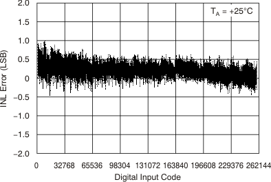
DAC9881 tc_5v_25c_inl_bas438.gif
Figure 4. Linearity Error vs Digital Input Code
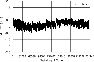
DAC9881 tc_5v_40c_inl_bas438.gif
Figure 6. Linearity Error vs Digital Input Code
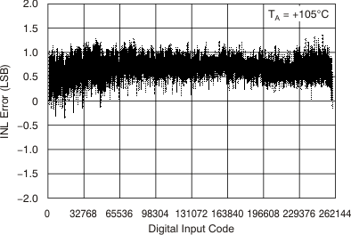
DAC9881 tc_5v_105c_inl_bas438.gif
Figure 8. Linearity Error vs Digital Input Code
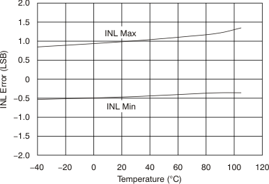
DAC9881 tc_5v_inl-tmp_bas438.gif
Figure 10. Linearity Error vs Temperature
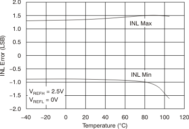
DAC9881 tc_5v_inl-tmp_2x_bas438.gif
Gain = 2X mode
Figure 12. Linearity Error vs Temperature
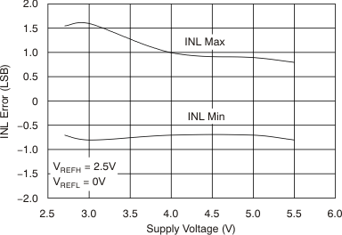
DAC9881 tc_5v_inl-vdd_bas438.gif
Figure 14. Linearity Error vs Supply Voltage
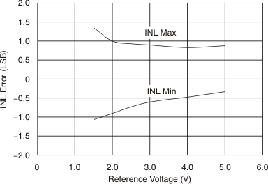
DAC9881 tc_5v_inl-vref_bas438.gif
Figure 16. Linearity Error vs Reference Voltage
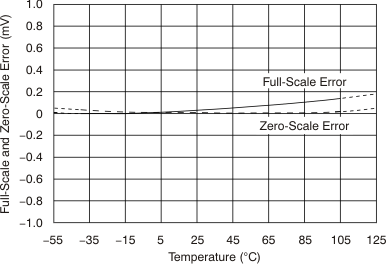
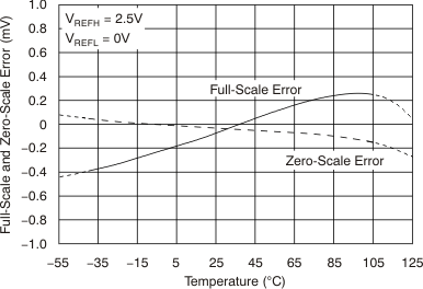
DAC9881 tc_5v_fs_zse-tmp_bas438.gif
Figure 18. Full-Scale and Zero-Scale Error vs Temperature
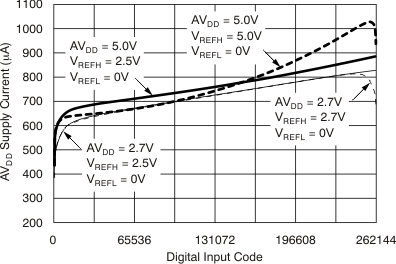
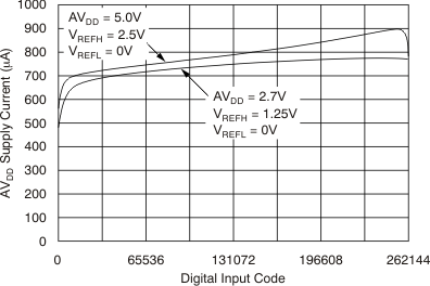
DAC9881 tc_5v_is-code_bas438.gif
Figure 20. AVDD Supply Current vs Digital Input Code
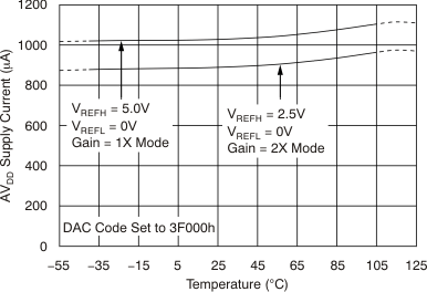
DAC9881 tc_5v_is-tmp_bas438.gif
Figure 22. AVDD Supply Current vs Temperature
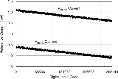
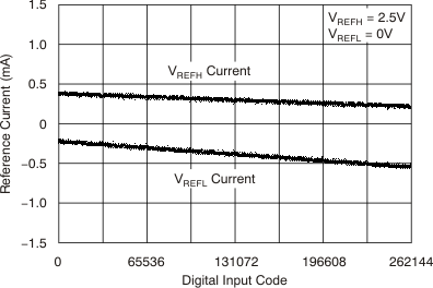
DAC9881 tc_5v_iref-code_bas438.gif
Figure 24. Reference Current vs Digital Input Code
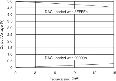
DAC9881 tc_5v_vo-dcc_bas438.gif
Figure 26. Output Voltage vs Drive Current Capability
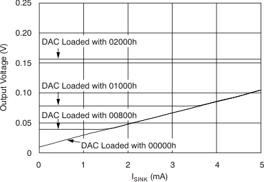
DAC9881 tc_5v_vo-dcc_agnd_bas438.gif
Figure 28. Output Voltage vs Drive Current Capability (Operation Near AGND Rail)
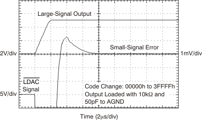
DAC9881 tc_5v_time_0-3f_bas438.gif
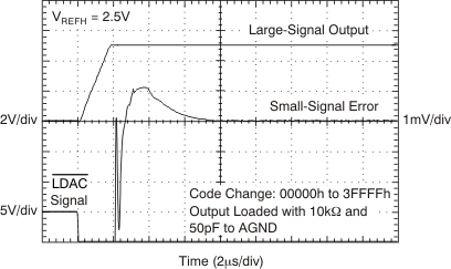
Figure 30. Large-Signal Settling Time
DAC9881 tc_5v_time_4-3c_bas438.gif
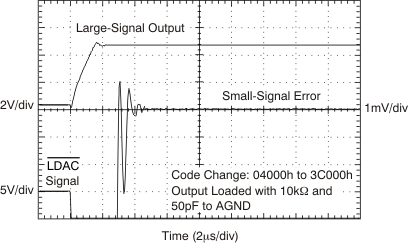
Figure 32. Large-Signal Settling Time
DAC9881 tc_5v_time_0-3f_2x_bas438.gif
Gain = 2X mode
Figure 34. Large-Signal Settling Time
DAC9881 tc_5v_time_4-3c_2x_bas438.gif
Gain = 2X mode
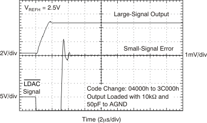
Figure 36. Large-Signal Settling Time
DAC9881 tc_5v_glch_1-2_5v_bas438.gif
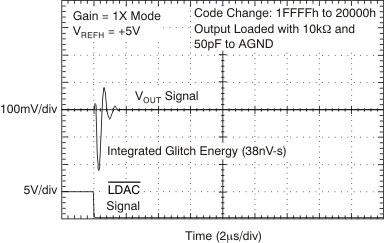
Figure 38. Major Carry Glitch
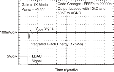
DAC9881 tc_5v_glch_1-2_25v_bas438.gif
Figure 40. Major Carry Glitch
DAC9881 tc_5v_noise-frq_bas438.gif
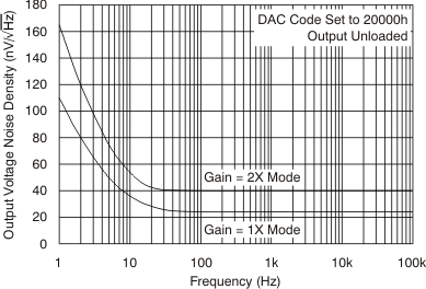
Figure 42. Output Noise Density vs Frequency
DAC9881 tc_5v_25c_dnl_bas438.gif
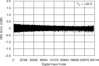
Figure 5. Differential Linearity Error vs Digital Input Code
DAC9881 tc_5v_40c_dnl_bas438.gif
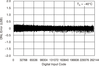
Figure 7. Differential Linearity Error vs Digital Input Code
DAC9881 tc_5v_105c_dnl_bas438.gif
Figure 9. Differential Lineary Error vs Digital Input Code
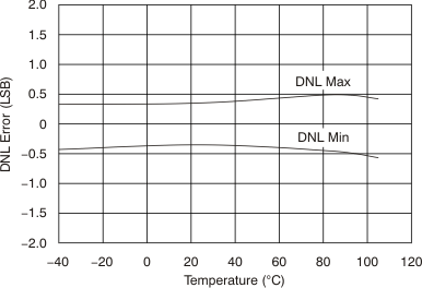
DAC9881 tc_5v_dnl-tmp_bas438.gif
Figure 11. Differential Linearity Error vs Temperature
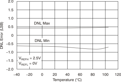
DAC9881 tc_5v_dnl-tmp_2x_bas438.gif
Gain = 2X mode
Figure 13. Differential Linearity Error vs Temperature
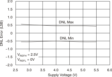
DAC9881 tc_5v_dnl-vdd_bas438.gif
Figure 15. Differential Linearity Error vs Supply Voltage
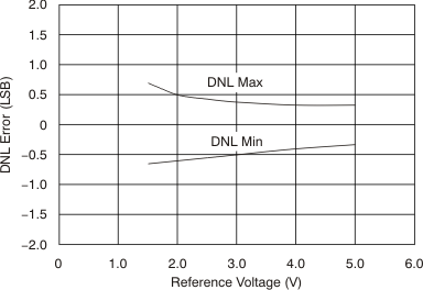
DAC9881 tc_5v_dnl-vref_bas438.gif
Figure 17. Differential Linearity Error vs Reference Voltage
DAC9881 tc_5v_fs_zse-tmp_2x_bas438.gif
Gain = 2X mode
Figure 19. Full-Scale and Zero-Scale Error vs Temperature
DAC9881 tc_5v_is-code_2x_bas438.gif
Gain = 2X mode
Figure 21. AVDD Supply Current vs Digital Input Code
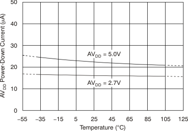
DAC9881 tc_5v_ipd-tmp_bas438.gif
Figure 23. AVDD Power-Down Current vs Temperature
DAC9881 tc_5v_iref-code_2x_bas438.gif
Gain = 2X mode
Figure 25. Reference Current vs Digital Input Code
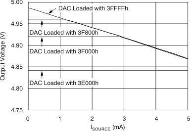
DAC9881 tc_5v_vo-dcc_avdd_bas438.gif
Figure 27. Output Voltage vs Drive Current Capability (Operation Near AVDD Rail)
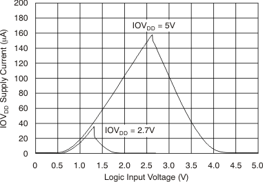
DAC9881 tc_5v_iovdd-logic_bas438.gif
Figure 29. IOVDD Supply Current vs Logic Input Voltage
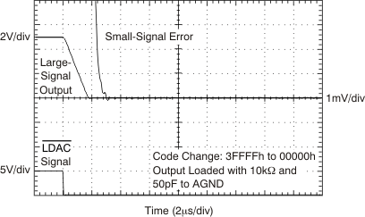
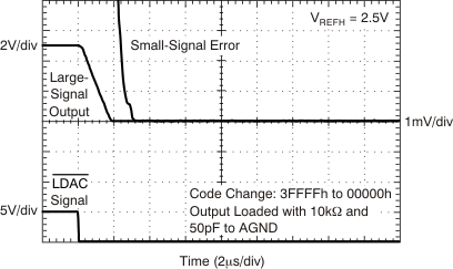
DAC9881 tc_5v_time_3f-0_bas438.gif
Figure 31. Large-Signal Settling Time
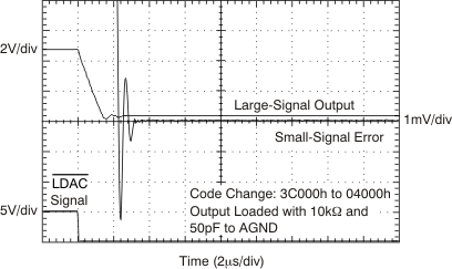
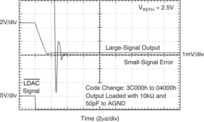
DAC9881 tc_5v_time_3c-4_bas438.gif
Figure 33. Large-Signal Settling Time
DAC9881 tc_5v_time_3f-0_2x_bas438.gif
Gain = 2X mode
Figure 35. Large-Signal Settling Time
DAC9881 tc_5v_time_3c-4_2x_bas438.gif
Gain = 2X mode
Figure 37. Large-Signal Settling Time
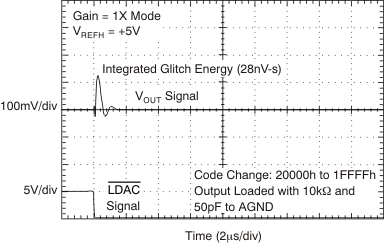
DAC9881 tc_5v_glch_2-1_5v_bas438.gif
Figure 39. Major Carry Glitch
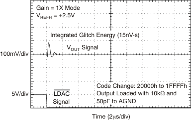
DAC9881 tc_5v_glch_2-1_25v_bas438.gif
Figure 41. Major Carry Glitch
DAC9881 tc_5v_lfo_noise_bas438.gif
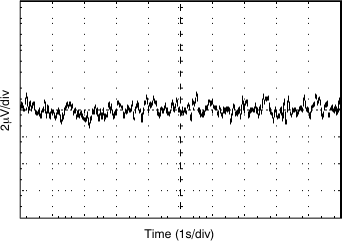
Figure 43. Low-Frequency Output Noise (0.1 Hz to 10 Hz)