SBVS013E October   2001  – July 2022 DCR010503 , DCR010505 , DCR011203 , DCR011205 , DCR012403 , DCR012405

PRODUCTION DATA  

  1. Features
  2. Applications
  3. Description
  4. Revision History
  5. Device Comparison Table
  6. Pin Configuration and Functions
  7. Specifications
    1. 7.1 Absolute Maximum Ratings
    2. 7.2 ESD Ratings
    3. 7.3 Recommended Operating Conditions
    4. 7.4 Thermal Information
    5. 7.5 Electrical Characteristics
    6. 7.6 Typical Characteristics
  8. Detailed Description
    1. 8.1 Overview
    2. 8.2 Functional Block Diagram
    3. 8.3 Feature Description
      1. 8.3.1  Isolation
        1. 8.3.1.1 Operation or Functional Isolation
        2. 8.3.1.2 Basic or Enhanced Isolation
        3. 8.3.1.3 Working Voltage
        4. 8.3.1.4 Isolation Voltage Rating
        5. 8.3.1.5 Repeated High-Voltage Isolation Testing
      2. 8.3.2  Power Stage
      3. 8.3.3  Rectification
      4. 8.3.4  Regulator
      5. 8.3.5  Oscillator and Watchdog
      6. 8.3.6  ERROR Flag
      7. 8.3.7  Synchronization
      8. 8.3.8  Construction
      9. 8.3.9  Thermal Considerations
      10. 8.3.10 Decoupling – Ripple Reduction
    4. 8.4 Device Functional Modes
      1. 8.4.1 Device Disable and Enable
      2. 8.4.2 Regulated Output Disable and Enable
  9. Application and Implementation
    1. 9.1 Application Information
      1. 9.1.1 DCR01 Single Voltage Output
      2. 9.1.2 Generating Two Positive Output Voltages
      3. 9.1.3 Generation of Dual Polarity Voltages from Two Self-Synchronized DCR01s
    2. 9.2 Typical Application
      1. 9.2.1 Design Requirements
      2. 9.2.2 Detailed Design Procedure
        1. 9.2.2.1 Input Capacitor
        2. 9.2.2.2 Output Capacitor
        3. 9.2.2.3 Filter Capacitor
        4. 9.2.2.4 ERROR Flag
      3. 9.2.3 Application Curves
  10. 10Power Supply Recommendations
  11. 11Layout
    1. 11.1 Layout Guidelines
    2. 11.2 Layout Examples
  12. 12Device and Documentation Support
    1. 12.1 Receiving Notification of Documentation Updates
    2. 12.2 Support Resources
    3. 12.3 Trademarks
    4. 12.4 Electrostatic Discharge Caution
    5. 12.5 Glossary
  13. 13Mechanical, Packaging, and Orderable Information

Package Options

Mechanical Data (Package|Pins)
Thermal pad, mechanical data (Package|Pins)
Orderable Information

Pin Configuration and Functions

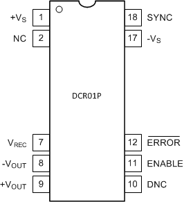
GUID-97306B49-0C24-486E-B697-87B49B19A8C1-low.gifFigure 6-1 10-Pin PDIPNVE Package(Top View)
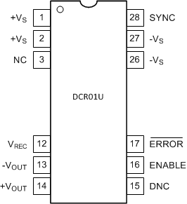
GUID-168625DD-3EAF-4503-A898-4C5DA044F0EA-low.gifFigure 6-2 12-Pin SOPDVB Package(Top View)
Table 6-1 Pin Functions
Pin I/O Description
Name PDIP SOP
ENABLE 11 16 I Output voltage enable
ERROR 12 17 O Error flag active low
DNC 10 15 Do not connect.
NC 2 3 No connection
SYNC 18 28 I Synchronization input
–VOUT 8 13 O Output ground
+VOUT 9 14 O Voltage output
VREC 7 12 O Rectified output
–VS 17 26, 27 I Input ground
+VS 1 1, 2 I Voltage input