DLPS183C March 2020 – March 2023 DLP3021-Q1
PRODUCTION DATA
- 1 Features
- 2 Applications
- 3 Description
- 4 Revision History
- 5 Pin Configuration and Functions
-
6 Specifications
- 6.1 Absolute Maximum Ratings
- 6.2 Storage Conditions
- 6.3 ESD Ratings
- 6.4 Recommended Operating Conditions
- 6.5 Thermal Information
- 6.6 Electrical Characteristics
- 6.7 Timing Requirements
- 6.8 Switching Characteristics
- 6.9 System Mounting Interface Loads
- 6.10 Physical Characteristics of the Micromirror Array
- 6.11 Micromirror Array Optical Characteristics
- 6.12 Window Characteristics
- 6.13 Chipset Component Usage Specification
- 7 Detailed Description
- 8 Application and Implementation
- 9 Power Supply Recommendations
- 10Layout
- 11Device and Documentation Support
- 12Mechanical, Packaging, and Orderable Information
Package Options
Mechanical Data (Package|Pins)
- FQR|54
Thermal pad, mechanical data (Package|Pins)
Orderable Information
7.3.7 DMD JTAG Interface
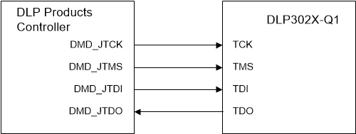
The DMD uses 4 standard JTAG signals for sending and receiving boundary scan test data. TCK is the test clock used to drive an IEEE 1149.1 TAP state machine and logic. TMS directs the next state of the TAP state machine. TDI is the scan data input and TDO is the scan data output.
The DMD does not support IEEE 1149.1 signals TRST (Test Logic Reset) and RTCK (Returned Test Clock). Boundary scan cells on the DMD are Observe-Only. To initiate the JTAG boundary scan operation on the DMD, a minimum of 6 TCK clock cycles are required after TMS is set to logic high.
Refer to Figure 7-4 for a JTAG system board routing example.
 Figure 7-4 System Interface Connection to DLP Products Controller
The DMD Device ID can be read via the JTAG interface. The ID and 32-bit shift order is shown in Figure 7-5.
 Figure 7-5 DMD Device ID and 32-bit Shift Order
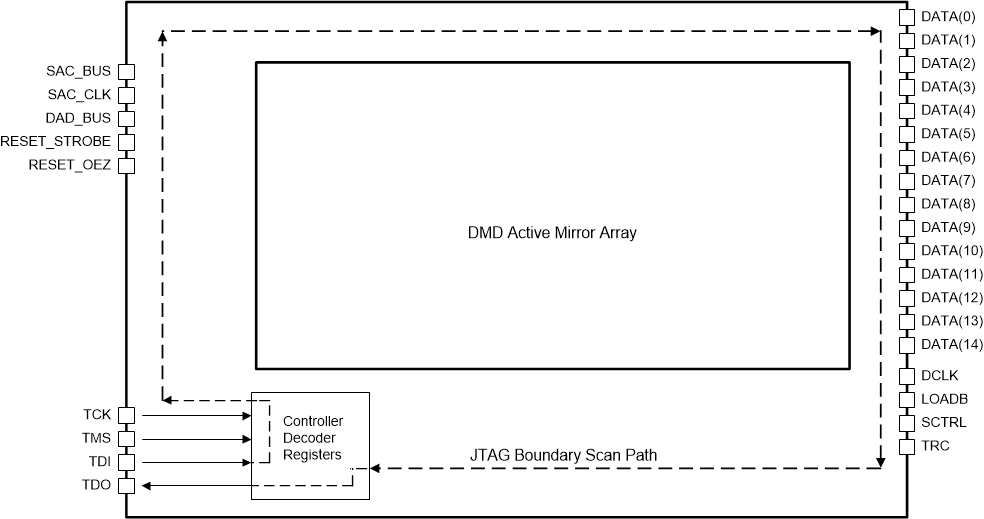
Refer to Figure 7-6 for a JTAG boundary scan block diagram for the DMD. These show the pins and the scan order that are observed during the JTAG boundary scan.
 Figure 7-6 JTAG Boundary Scan Path
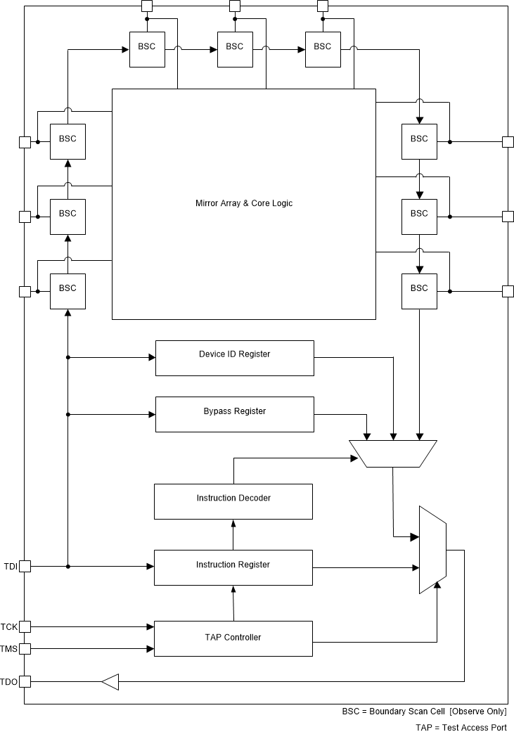
Refer to Figure 7-7 for a functional block diagram of the JTAG control logic.
 Figure 7-7 JTAG Functional Block Diagram