DLPS183C March 2020 – March 2023 DLP3021-Q1
PRODUCTION DATA
- 1 Features
- 2 Applications
- 3 Description
- 4 Revision History
- 5 Pin Configuration and Functions
-
6 Specifications
- 6.1 Absolute Maximum Ratings
- 6.2 Storage Conditions
- 6.3 ESD Ratings
- 6.4 Recommended Operating Conditions
- 6.5 Thermal Information
- 6.6 Electrical Characteristics
- 6.7 Timing Requirements
- 6.8 Switching Characteristics
- 6.9 System Mounting Interface Loads
- 6.10 Physical Characteristics of the Micromirror Array
- 6.11 Micromirror Array Optical Characteristics
- 6.12 Window Characteristics
- 6.13 Chipset Component Usage Specification
- 7 Detailed Description
- 8 Application and Implementation
- 9 Power Supply Recommendations
- 10Layout
- 11Device and Documentation Support
- 12Mechanical, Packaging, and Orderable Information
Package Options
Mechanical Data (Package|Pins)
- FQR|54
Thermal pad, mechanical data (Package|Pins)
Orderable Information
7.3.6 Temperature Sensing Diode
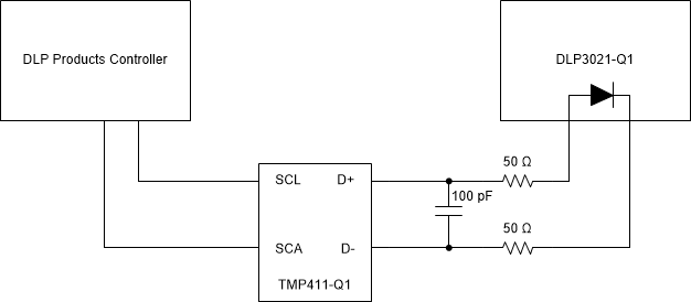
The DMD includes a temperature sensing diode designed to be used with the TMP411-Q1 temperature monitoring device. The DLP products controller may monitor the DMD array temperature via the TMP411-Q1 and temperature sense diode.
Figure 7-1 shows the typical connection between the DLP products controller, TMP411-Q1, and the DLP3021-Q1 DMD. The signals to the temperature sense diode are sensitive to system noise, and care should be taken in the routing and implementation of this circuit. See the TMP411-Q1 data sheet for detailed PCB layout recommendations.
 Figure 7-1 Temperature Sense Diode Typical Circuit Configuration
It is recommended that the host controller manage parking of the DMD based on the allowable temperature specifications and temperature measurements.