DLPS076B November 2017 – June 2019 DLP3030-Q1
PRODUCTION DATA.
- 1 Features
- 2 Applications
- 3 Description
- 4 Revision History
- 5 Pin Configuration and Functions
-
6 Specifications
- 6.1 Absolute Maximum Ratings
- 6.2 Storage Conditions
- 6.3 ESD Ratings
- 6.4 Recommended Operating Conditions
- 6.5 Thermal Information
- 6.6 Electrical Characteristics
- 6.7 Timing Requirements
- 6.8 Switching Characteristics
- 6.9 System Mounting Interface Loads
- 6.10 Physical Characteristics of the Micromirror Array
- 6.11 Optical Characteristics of the Micromirror Array
- 6.12 Window Characteristics
- 6.13 Chipset Component Usage Specification
- 7 Detailed Description
- 8 Application and Implementation
- 9 Power Supply Recommendations
- 10Layout
- 11Device and Documentation Support
- 12Mechanical, Packaging, and Orderable Information
Package Options
Mechanical Data (Package|Pins)
- FYJ|149
Thermal pad, mechanical data (Package|Pins)
Orderable Information
11.1.2 Device Markings
The device marking is shown below. The marking will include both human-readable information and a 2-dimensional matrix code.
The human-readable information is described below. The 2-dimensional matrix code is an alpha-numeric character string that contains the DMD part number, part 1 of serial number, and part 2 of serial number.
The first character of the DMD serial number (part 1) is the manufacturing year. The second character of the DMD serial number (part 1) is the manufacturing month. The last character of the DMD serial number (part 2) is the bias voltage bin letter.
Example: *DLP3030AFYJQ1 GHXXXXX LLLLLLM
 Figure 20. DMD Marking
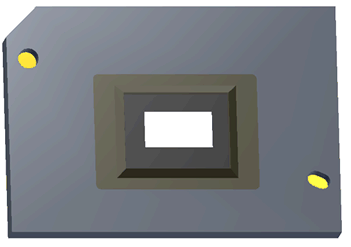
 A 3-dimensional modeled depiction of the DLP3030-Q1 device is shown below.
 Figure 21. Image of DLP3030-Q1