DLPS200B July 2020 – April 2021 DLP5530S-Q1
PRODUCTION DATA
- 1 Features
- 2 Applications
- 3 Description
- 4 Revision History
- 5 Pin Configuration and Functions
-
6 Specifications
- 6.1 Absolute Maximum Ratings
- 6.2 Storage Conditions
- 6.3 ESD Ratings
- 6.4 Recommended Operating Conditions
- Illumination Overfill Diagram
- 6.5 Thermal Information
- 6.6 Electrical Characteristics
- 6.7 Timing Requirements
- Electrical and Timing Diagrams
- 6.8 Switching Characteristics
- LPSDR and Test Load Circuit Diagrams
- 6.9 System Mounting Interface Loads
- System Interface Loads Diagram
- 6.10 Physical Characteristics of the Micromirror Array
- Array Physical Characteristics Diagram
- 6.11 Micromirror Array Optical Characteristics
- 6.12 Window Characteristics
- 6.13 Chipset Component Usage Specification
- 7 Detailed Description
- 8 Application and Implementation
- 9 Power Supply Recommendations
- 10Layout
- 11Device and Documentation Support
- 12Mechanical, Packaging, and Orderable Information
Package Options
Refer to the PDF data sheet for device specific package drawings
Mechanical Data (Package|Pins)
- FYS|149
Thermal pad, mechanical data (Package|Pins)
Orderable Information
8.2 Typical Application
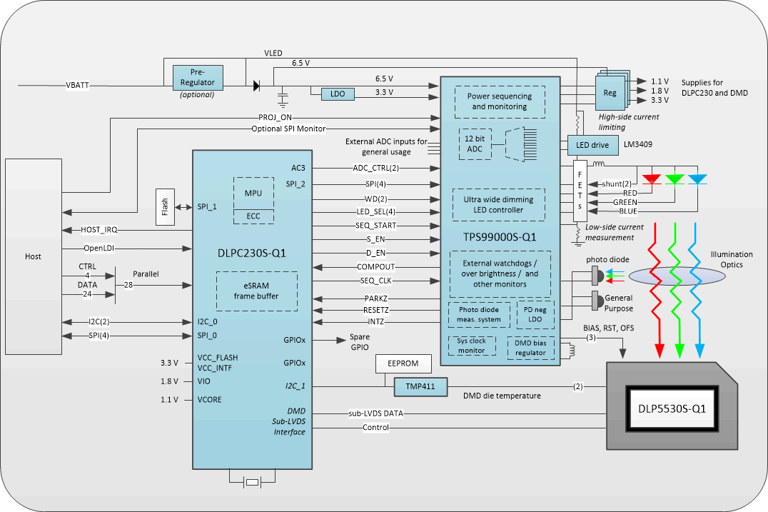
The chipset consists of three components—the DLP5530S-Q1 automotive DMD, the DLPC230S-Q1, and the TPS99000S-Q1. The DMD is a light modulator consisting of tiny mirrors that are used to form and project images. The DLPC230S-Q1 is a controller for the DMD; it formats incoming video and controls the timing of the DMD illumination sources and the DMD in order to display the incoming video. The TPS99000S-Q1 is a controller for the illumination sources (e.g. LEDs or lasers) and a management IC for the entire chipset. In conjunction, the DLPC230S-Q1 and the TPS99000S-Q1 can also be used for system-level monitoring, diagnostics, and failure detection features. Figure 8-1 is a system level block diagram with these devices in the DLP head-up display configuration and shows the primary features and functions of each device.
 Figure 8-1 Head-Up Display System Block
Diagram