DLPS075G April   2016  – May 2019 DLP5531-Q1

PRODUCTION DATA.  

  1. Features
  2. Applications
  3. Description
    1.     Device Images
      1.      DLP5531-Q1 DLP Chipset System Block Diagram
  4. Revision History
  5. Pin Configuration and Functions
    1.     Pin Functions – Connector Pins
    2.     Pin Functions – Test Pads
  6. Specifications
    1. 6.1  Absolute Maximum Ratings
    2. 6.2  Storage Conditions
    3. 6.3  ESD Ratings
    4. 6.4  Recommended Operating Conditions
    5. 6.5  Thermal Information
    6. 6.6  Electrical Characteristics
    7. 6.7  Timing Requirements
    8. 6.8  Switching Characteristics
    9. 6.9  System Mounting Interface Loads
    10. 6.10 Physical Characteristics of the Micromirror Array
    11. 6.11 Micromirror Array Optical Characteristics
    12. 6.12 Window Characteristics
    13. 6.13 Chipset Component Usage Specification
  7. Detailed Description
    1. 7.1 Overview
    2. 7.2 Functional Block Diagram
    3. 7.3 Feature Description
      1. 7.3.1 Sub-LVDS Data Interface
      2. 7.3.2 Low Speed Interface for Control
      3. 7.3.3 DMD Voltage Supplies
      4. 7.3.4 Asynchronous Reset
      5. 7.3.5 Temperature Sensing Diode
        1. 7.3.5.1 Temperature Sense Diode Theory
    4. 7.4 System Optical Considerations
      1. 7.4.1 Numerical Aperture and Stray Light Control
      2. 7.4.2 Pupil Match
      3. 7.4.3 Illumination Overfill
    5. 7.5 DMD Image Performance Specification
    6. 7.6 Micromirror Array Temperature Calculation
      1. 7.6.1 Temperature Rise Through the Package for Heatsink Design
      2. 7.6.2 Monitoring Array Temperature Using the Temperature Sense Diode
    7. 7.7 Micromirror Landed-On/Landed-Off Duty Cycle
      1. 7.7.1 Definition of Micromirror Landed-On/Landed-Off Duty Cycle
  8. Application and Implementation
    1. 8.1 Application Information
    2. 8.2 Typical Application
      1. 8.2.1 Application Overview
      2. 8.2.2 Reference Design
      3. 8.2.3 Application Mission Profile Consideration
  9. Power Supply Recommendations
    1. 9.1 Power Supply Power-Up Procedure
    2. 9.2 Power Supply Power-Down Procedure
    3. 9.3 Power Supply Sequencing Requirements
  10. 10Layout
    1. 10.1 Layout Guidelines
  11. 11Device and Documentation Support
    1. 11.1 Device Support
      1. 11.1.1 Device Nomenclature
      2. 11.1.2 Device Markings
    2. 11.2 Related Links
    3. 11.3 Community Resources
    4. 11.4 Trademarks
    5. 11.5 Electrostatic Discharge Caution
    6. 11.6 DMD Handling
    7. 11.7 Glossary
  12. 12Mechanical, Packaging, and Orderable Information

Package Options

Refer to the PDF data sheet for device specific package drawings

Mechanical Data (Package|Pins)
  • FYK|149
Thermal pad, mechanical data (Package|Pins)
Orderable Information

System Mounting Interface Loads

PARAMETER MIN NOM MAX UNIT
Condition 1: Maximum load evenly distributed within each area(1)
Thermal Interface Area 110.8 N
Electrical Interface Area 111.3
Condition 2: Maximum load evenly distributed within each area(1)
Thermal Interface Area 0 N
Electrical Interface Area 222.1
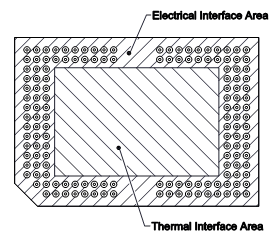
See Figure 12.
DLP5531-Q1 auto_g2_mech_loads.gifFigure 12. System Interface Loads