DLPS177A September 2019 – November 2019 DLP5534-Q1
PRODUCTION DATA.
- 1 Features
- 2 Applications
- 3 Description
- 4 Revision History
- 5 Pin Configuration and Functions
-
6 Specifications
- 6.1 Absolute Maximum Ratings
- 6.2 Storage Conditions
- 6.3 ESD Ratings
- 6.4 Recommended Operating Conditions
- 6.5 Thermal Information
- 6.6 Electrical Characteristics
- 6.7 Timing Requirements
- 6.8 Switching Characteristics
- 6.9 System Mounting Interface Loads
- 6.10 Physical Characteristics of the Micromirror Array
- 6.11 Micromirror Array Optical Characteristics
- 6.12 Window Characteristics
- 6.13 Chipset Component Usage Specification
- 7 Detailed Description
- 8 Application and Implementation
- 9 Power Supply Recommendations
- 10Layout
- 11Device and Documentation Support
- 12Mechanical, Packaging, and Orderable Information
Package Options
Mechanical Data (Package|Pins)
- FYK|149
Thermal pad, mechanical data (Package|Pins)
Orderable Information
6.4 Recommended Operating Conditions
Over operating free-air temperature range (unless otherwise noted)(1)(2)| MIN | NOM | MAX | UNIT | |||
|---|---|---|---|---|---|---|
| SUPPLY VOLTAGE RANGE(3) | ||||||
| VDD | Supply voltage for LVCMOS core logic
Supply voltage for LPSDR low-speed interface |
1.7 | 1.8 | 1.95 | V | |
| VDDI | Supply voltage for SubLVDS receivers | 1.7 | 1.8 | 1.95 | V | |
| VOFFSET | Supply voltage for HVCMOS and micromirror electrode(4) | 8.25 | 8.5 | 8.75 | V | |
| VBIAS | Supply voltage for mirror electrode | 15.5 | 16 | 16.5 | V | |
| VRESET | Supply voltage for micromirror electrode | –9.5 | –10 | –10.5 | V | |
| | VDDI–VDD | | Supply voltage delta (absolute value)(5) | 0.3 | V | |||
| | VBIAS–VOFFSET | | Supply voltage delta (absolute value)(6) | 8.75 | V | |||
| CLOCK FREQUENCY | ||||||
| ƒclock | Clock frequency for low speed interface LS_CLK | 120 | MHz | |||
| ƒclock | Clock frequency for high speed interface DCLK(7) | 600 | MHz | |||
| Duty cycle distortion DCLK | 44% | 56% | ||||
| SUBLVDS INTERFACE(7) | ||||||
| | VID | | SubLVDS input differential voltage (absolute value;
see Figure 6, Figure 7) |
150 | 250 | 350 | mV | |
| VCM | Common mode voltage (see Figure 6, Figure 7) | 700 | 900 | 1100 | mV | |
| VSUBLVDS | SubLVDS voltage (see Figure 6, Figure 7) | 575 | 1225 | mV | ||
| ZLINE | Line differential impedance (PWB/trace) | 90 | 100 | 110 | Ω | |
| ZIN | Internal differential termination resistance (see Figure 8) | 80 | 100 | 120 | Ω | |
| TEMPERATURE DIODE | ||||||
| ITEMP_DIODE | Max current source into Temperature Diode(8) | 120 | µA | |||
| ENVIRONMENTAL | ||||||
| TARRAY | Operating DMD array temperature(9) | –40 | 105 | °C | ||
| ILLsub-385nm | Illumination, wavelength < 385 nm | 2 | mW/cm2 | |||
| ILL385-to-395nm | Illumination, 385 nm < wavelength < 395 nm | 250 | mW/cm2 | |||
| ILL395-to-400nm | Illumination, 395 nm < wavelength < 400 nm | 800 | mW/cm2 | |||
| ILL400-to-420nm | Illumination, 400 nm < wavelength < 420 nm | 8 | W/cm2 | |||
| ILLVIS | Illumination, 420 nm < wavelength < 800 nm | Thermally limited(10) | W/cm2 | |||
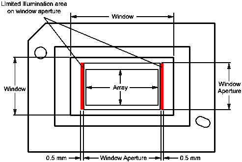
| ILLOVERFILL | Illumination overfill maximum heat load in areas shown in Figure 1(11) | TARRAY ≤ 75°C | 40 | mW/mm2 | ||
| Illumination overfill maximum heat load in areas shown in Figure 1(11) | TARRAY > 75°C | 29 | ||||
(1) The following power supplies are all required to operate the DMD: VDD, VDDI, VOFFSET, VBIAS, and VRESET. All VSS connections are also required.
(2) Recommended Operating Conditions are applicable after the DMD is installed in the final product.
(3) All voltage values are with respect to the ground pins (VSS).
(4) VOFFSET supply transients must fall within specified max voltages.
(5) To prevent excess current, the supply voltage delta |VDDI – VDD| must be less than the specified limit.
(6) To prevent excess current, the supply voltage delta |VBIAS – VOFFSET| must be less than the specified limit.
(7) Refer to the SubLVDS timing requirements in Timing Requirements.
(8) Temperature Diode is to allow accurate measurement of the DMD array temperature during operation.
(9) DMD active array temperature can be calculated as shown in Micromirror Array Temperature Calculation section. Additionally, the DMD array temperature is monitored in the system using the TMP411-Q1 and DLPC230-Q1 as shown in the system block diagram.
(10) Limited by the resulting micromirror array temperature. Refer to the calculation example in Micromirror Array Temperature Calculation section.
(11) The active area of the DLP5534-Q1 device is surrounded by an aperture on the inside of the DMD window surface that masks structures of the DMD device assembly from normal view. The aperture is sized to anticipate several optical conditions. Overfill light illuminating the area outside the active array can scatter and create adverse effects to the performance of an end application using the DMD. The illumination optical system should be designed to minimize light flux incident outside the active array. Depending on the particular system's optical architecture and assembly tolerances, the amount of overfill light on the outside of the active array may cause system performance degradation.
 Figure 1. Illumination Overfill Diagram