DLPS136 November 2018 DLP650LNIR
PRODUCTION DATA.
- 1 Features
- 2 Applications
- 3 Description
- 4 Revision History
- 5 Pin Configuration and Functions
-
6 Specifications
- 6.1 Absolute Maximum Ratings
- 6.2 Storage Conditions
- 6.3 ESD Ratings
- 6.4 Recommended Operating Conditions
- 6.5 Thermal Information
- 6.6 Electrical Characteristics
- 6.7 Timing Requirements
- 6.8 System Mounting Interface Loads
- 6.9 Micromirror Array Physical Characteristics
- 6.10 Micromirror Array Optical Characteristics
- 6.11 Window Characteristics
- 6.12 Chipset Component Usage Specification
-
7 Detailed Description
- 7.1 Overview
- 7.2 System Functional Block Diagram
- 7.3
Feature Description
- 7.3.1 DLPC410: Digital Controller for DLP Discovery 4100 Chipset
- 7.3.2 DLPA200: DMD Micromirror Driver
- 7.3.3 DLPR410: PROM for DLP Discovery 4100 Chipset
- 7.3.4 DLP650LNIR: DLP 0.65 WXGA NIR 2xLVDS Series 450 DMD
- 7.3.5 Measurement Conditions
- 7.4 Device Operational Modes
- 7.5 Feature Description
- 7.6 Optical Interface and System Image Quality Considerations
- 7.7 Micromirror Temperature Calculations
- 7.8 Micromirror Landed-On/Landed-Off Duty Cycle
- 8 Application and Implementation
- 9 Power Supply Recommendations
- 10Layout
- 11Device and Documentation Support
- 12Mechanical, Packaging, and Orderable Information
Package Options
Mechanical Data (Package|Pins)
- FYL|149
Thermal pad, mechanical data (Package|Pins)
Orderable Information
7.3.4.1.3.2 DLPC410 to DLPA200 IO Description
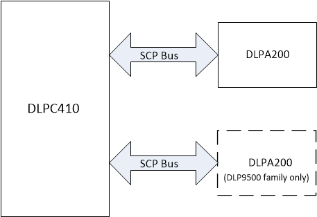
The Serial Communications Port (SCP) is a full duplex, synchronous, character-oriented (byte) port that allows exchange of commands from the DLPC410 to the DLPA200. One SCP bus is used for the DLP650LNIR.
 Figure 13. Serial Port System Configuration
 Five signal lines are associated with the SCP bus: SCPEN, SCPCK, SCPDI, SCPDO, and IRQ.
Table 6 lists the available controls and status pin names and their corresponding signal type, along with a brief functional description.
Table 6. DLPC410 to DLPA200 I/O Pin Descriptions
| PIN NAME | DESCRIPTION | I/O |
|---|---|---|
| A_SCPEN | Active-low chip select for DLPA200 serial bus | O |
| A_STROBE | DLPA200 control signal strobe | O |
| A_MODE(1:0) | DLPA200 mode control | O |
| A_SEL(1:0) | DLPA200 select control | O |
| A_ADDR(3:0) | DLPA200 address control | O |
| B_SCPEN | Active-low chip select for DLPA200 serial bus (2) | O |
| B_STROBE | DLPA200 control signal strobe (2) | O |
| B_MODE(1:0) | DLPA200 mode control | O |
| B_SEL(1:0) | DLPA200 select control | O |
| B_ADDR(3:0) | DLPA200 address control | O |
The DLPA200 provides a variety of output options to the DMD by selecting logic control inputs: MODE[1:0], SEL[1:0] and reset group address A[3:0] (Table 6). The MODE[1:0] input determines whether a single output, two outputs, four outputs, or all outputs, are selected. Output levels (VBIAS, VOFFSET, or VRESET) are selected by SEL[1:0] pins. Selected outputs are tri-stated on the rising edge of the STROBE signal and latched to the selected voltage level after a break-before-make delay. Outputs remain latched at the last micromirror clocking pulse waveform level until the next micromirror clocking pulse waveform cycle.