DLPS136 November   2018 DLP650LNIR

PRODUCTION DATA.  

  1. Features
  2. Applications
  3. Description
    1.     Device Images
      1.      Simplified Application
  4. Revision History
  5. Pin Configuration and Functions
    1.     Pin Functions
  6. Specifications
    1. 6.1  Absolute Maximum Ratings
    2. 6.2  Storage Conditions
    3. 6.3  ESD Ratings
    4. 6.4  Recommended Operating Conditions
    5. 6.5  Thermal Information
    6. 6.6  Electrical Characteristics
    7. 6.7  Timing Requirements
    8. 6.8  System Mounting Interface Loads
    9. 6.9  Micromirror Array Physical Characteristics
    10. 6.10 Micromirror Array Optical Characteristics
    11. 6.11 Window Characteristics
    12. 6.12 Chipset Component Usage Specification
  7. Detailed Description
    1. 7.1 Overview
    2. 7.2 System Functional Block Diagram
    3. 7.3 Feature Description
      1. 7.3.1 DLPC410: Digital Controller for DLP Discovery 4100 Chipset
      2. 7.3.2 DLPA200: DMD Micromirror Driver
      3. 7.3.3 DLPR410: PROM for DLP Discovery 4100 Chipset
      4. 7.3.4 DLP650LNIR: DLP 0.65 WXGA NIR 2xLVDS Series 450 DMD
        1. 7.3.4.1 DLP650LNIR Chipset Interfaces
          1. 7.3.4.1.1 DLPC410 Interface Description
            1. 7.3.4.1.1.1 DLPC410 IO
            2. 7.3.4.1.1.2 Initialization
            3. 7.3.4.1.1.3 DMD Device Detection
            4. 7.3.4.1.1.4 Power Down
          2. 7.3.4.1.2 DLPC410 to DMD Interface
            1. 7.3.4.1.2.1 DLPC410 to DMD IO Description
            2. 7.3.4.1.2.2 Data Flow
          3. 7.3.4.1.3 DLPC410 to DLPA200 Interface
            1. 7.3.4.1.3.1 DLPA200 Operation
            2. 7.3.4.1.3.2 DLPC410 to DLPA200 IO Description
          4. 7.3.4.1.4 DLPA200 to DLP650LNIR Interface
            1. 7.3.4.1.4.1 DLPA200 to DLP650LNIR Interface Overview
      5. 7.3.5 Measurement Conditions
    4. 7.4 Device Operational Modes
      1. 7.4.1 DMD Block Modes
        1. 7.4.1.1 Single Block Mode
        2. 7.4.1.2 Dual Block Mode
        3. 7.4.1.3 Quad Block Mode
        4. 7.4.1.4 Global Mode
      2. 7.4.2 DMD Load4 Mode
    5. 7.5 Feature Description
      1. 7.5.1 Power Interface
      2. 7.5.2 Timing
    6. 7.6 Optical Interface and System Image Quality Considerations
      1. 7.6.1 Optical Interface and System Image Quality
      2. 7.6.2 Numerical Aperture and Stray Light Control
      3. 7.6.3 Pupil Match
      4. 7.6.4 Illumination Overfill
    7. 7.7 Micromirror Temperature Calculations
      1. 7.7.1 Sample Calculation 1: Uniform Illumination of Entire DMD Active Array (1280 × 800 pixels)
      2. 7.7.2 Sample Calculation 2: Partial DMD Active Array Illumination with Non-uniform Illumination Peak
    8. 7.8 Micromirror Landed-On/Landed-Off Duty Cycle
      1. 7.8.1 Definition of Micromirror Landed-On/Landed-Off Duty Cycle
      2. 7.8.2 Landed Duty Cycle and Useful Life of the DMD
      3. 7.8.3 Landed Duty Cycle and Operational DMD Temperature
      4. 7.8.4 Estimating the Long-Term Average Landed Duty Cycle of a Product or Application
  8. Application and Implementation
    1. 8.1 Application Information
      1. 8.1.1 Device Description
    2. 8.2 Typical Application
      1. 8.2.1 Design Requirements
      2. 8.2.2 Detailed Design Procedure
  9. Power Supply Recommendations
  10. 10Layout
    1. 10.1 Layout Guidelines
      1. 10.1.1 Impedance Requirements
      2. 10.1.2 PCB Signal Routing
      3. 10.1.3 Fiducials
      4. 10.1.4 DMD Interface
        1. 10.1.4.1 Trace Length Matching
      5. 10.1.5 DLP650LNIR Decoupling
        1. 10.1.5.1 Decoupling Capacitors
      6. 10.1.6 VCC and VCC2
      7. 10.1.7 DMD Layout
      8. 10.1.8 DLPA200
    2. 10.2 Layout Example
  11. 11Device and Documentation Support
    1. 11.1 Device Support
      1. 11.1.1 Device Nomenclature
      2. 11.1.2 Device Markings
    2. 11.2 Documentation Support
      1. 11.2.1 Related Documentation
    3. 11.3 Related Links
    4. 11.4 Receiving Notification of Documentation Updates
    5. 11.5 Community Resources
    6. 11.6 Trademarks
    7. 11.7 Electrostatic Discharge Caution
    8. 11.8 Glossary
  12. 12Mechanical, Packaging, and Orderable Information

Package Options

Mechanical Data (Package|Pins)
Thermal pad, mechanical data (Package|Pins)
Orderable Information

Measurement Conditions

The data sheet provides timing at the device pin. For output timing analysis, the tester pin electronics and its transmission line effects must be taken into account. Figure 14 shows an equivalent test load circuit for the output under test. The load capacitance value stated is only for characterization and measurement of AC timing signals. This load capacitance value does not indicate the maximum load the DMD is capable of driving. All rise and fall transition timing parameters are referenced to VIL(max) and VIH(min) for input clocks, VOL(max) and VOH(min) for output clocks.
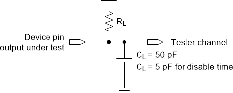
DLP650LNIR test_load_circuit.gifFigure 14. Test Load Circuit for AC Timing Measurements
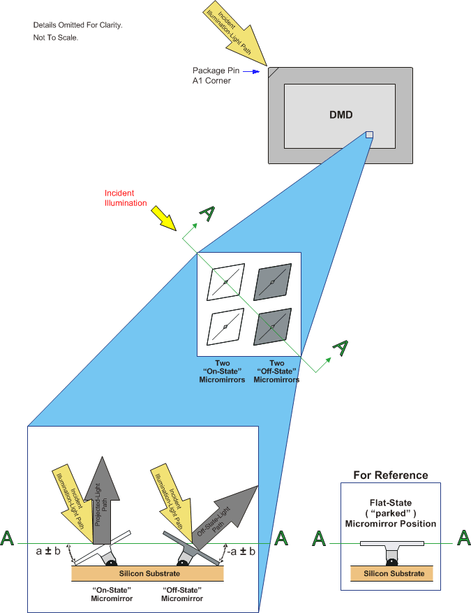
DLP650LNIR Micromirror_States_On_Off_Flat.gifFigure 15. Micromirror Landed Positions and Light Paths