DLPS082 February   2017 DLPA100

PRODUCTION DATA.  

  1. Features
  2. Applications
  3. Description
    1. 3.1 Typical Application Diagram
  4. Revision History
  5. Pin Configuration and Functions
    1.     Pin Functions
  6. Specifications
    1. 6.1 Absolute Maximum Ratings
    2. 6.2 Storage Conditions
    3. 6.3 ESD Ratings
    4. 6.4 Recommended Operating Conditions
    5. 6.5 Thermal Information
    6. 6.6 Electrical Characteristics
  7. Detailed Description
    1. 7.1 Overview
    2. 7.2 Functional Block Diagram
    3. 7.3 Feature Description
      1. 7.3.1  Power Up Sequencing
      2. 7.3.2  Power Down Sequencing
      3. 7.3.3  Shutdown
        1. 7.3.3.1 Thermal
      4. 7.3.4  System Reset
      5. 7.3.5  Interrupt Logic
      6. 7.3.6  Serial Communications Port
      7. 7.3.7  Switching Regulators
        1. 7.3.7.1 Output Voltage - VOUT
        2. 7.3.7.2 Adjustable Linear Regulator - VLIN1
        3. 7.3.7.3 Adjustable Linear Regulator Control - VLIN2
      8. 7.3.8  Fan Controllers
      9. 7.3.9  Color Wheel Motor Driver
        1. 7.3.9.1 Color Wheel Motor Driver Power Dissipation
      10. 7.3.10 Color Wheel Switching Regulator Supply
    4. 7.4 Device Functional Modes
  8. Application and Implementation
    1. 8.1 Application Information
    2. 8.2 Typical Application
      1. 8.2.1 Design Requirements
      2. 8.2.2 Detailed Design Procedure
      3. 8.2.3 Application Curves
  9. Power Supply Recommendations
  10. 10Layout
    1. 10.1 Layout Guidelines
    2. 10.2 Grounding Guidelines
      1. 10.2.1 Completely Isolated Ground Regions
      2. 10.2.2 Single Isolated Ground Region
      3. 10.2.3 Non-isolated Common Ground Region
    3. 10.3 Thermal Guidelines
    4. 10.4 Motor Control Guidelines
    5. 10.5 Layout Example
  11. 11Device and Documentation Support
    1. 11.1 Device Markings
    2. 11.2 Documentation Support
      1. 11.2.1 Related Documentation
    3. 11.3 Community Resources
    4. 11.4 Trademarks
    5. 11.5 Electrostatic Discharge Caution
    6. 11.6 Glossary
  12. 12Mechanical, Packaging, and Orderable Information
    1. 12.1 Package Option Addendum
      1. 12.1.1 Packaging Information

Package Options

Mechanical Data (Package|Pins)
  • DLP|48
Thermal pad, mechanical data (Package|Pins)

Power Down Sequencing

If VBB drops below the undervoltage level (VBBuvlo), the PWRGOOD will flag. If VBB drops below the undervoltage level (VBBuvsd), all the switcher and linear channels will turn off and the output rails will be supplied by the output filter capacitors. The duration between VBBuvlo and VBBuvsd allows sufficient ‘hold up’ time to ‘park’ the DMD mirrors. Although the regulators can supply rated current down to VBBuvsd, they can only provide this power for a maximum of 0.5 ms.

If either of the rails: VCORE or V3P3 or V2P5 drop below their respective undervoltage levels, the POSENSE and PWRGOOD will flag immediately.
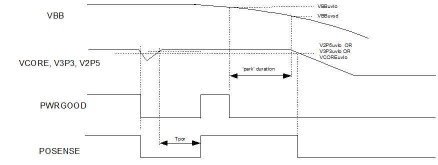
DLPA100 DLPA100_powerdown_sequencing.jpgFigure 2. Power Down Sequencing Timing Diagram