DLPS082 February 2017 DLPA100
PRODUCTION DATA.
- 1 Features
- 2 Applications
- 3 Description
- 4 Revision History
- 5 Pin Configuration and Functions
- 6 Specifications
-
7 Detailed Description
- 7.1 Overview
- 7.2 Functional Block Diagram
- 7.3 Feature Description
- 7.4 Device Functional Modes
- 8 Application and Implementation
- 9 Power Supply Recommendations
- 10Layout
- 11Device and Documentation Support
- 12Mechanical, Packaging, and Orderable Information
Package Options
Mechanical Data (Package|Pins)
- DLP|48
Thermal pad, mechanical data (Package|Pins)
7.3.6 Serial Communications Port
The Serial communications port (SCP) is a full duplex, synchronous, character-oriented byte port that allows exchange of data between the DLP controller (master) and the DLPA100.
Table 1. Serial Communications Port Signal Definitions
| SIGNAL | I/O | FROM/TO | TYPE | DESCRIPTION |
|---|---|---|---|---|
| SCPK | I | SCP bus master to slave | LVTTL compatible | SCP bus serial transfer clock. The host processor (master) generates this clock. |
| SCPENZ | I | SCP bus master to slave | LVTTL compatible | SCP bus access enable (low true). When high, slave will reset to idle state, and SCPDO output will tri-state. Pulling SCPENZ low initiates a read or write access. SCPENZ must remain low for an entire read/write access, and must be pulled high after the last data cycle. To abort a read or write cycle, pull SCPENZ high at any point. |
| SCPDI | I | SCP bus master to slave | LVTTL compatible | SCP bus serial data input. Data bits are valid and must be clocked in on the falling edge of SCPCK. |
| SCPDO | O | SCP bus slave to master | LVTTL open drain w/tri-state | SCP bus serial data output. Data bits must clocked out on the rising edge of SCPCK. |
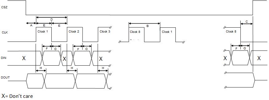
Table 2. Serial Interface Timing Requirements
| SYMBOL | CHARACTERISTICS | TEST CONDITIONS | MIN | NOM | MAX | UNIT |
|---|---|---|---|---|---|---|
| A | Setup CSZ low to CLK | Reference to rising edge of CLK | 360 | ns | ||
| B | Byte to Byte Delay | Nominally 1 CLK cycle rising edge to rising edge | 1.9 | µs | ||
| C | Setup DIN to CSZ High | Last byte to slave disable | 360 | ns | ||
| CLK Frequency | 0 | 526 | kHz | |||
| D | CLK Period | 1.9 | 2 | µs | ||
| E | CLK High or Low Time | 300 | ns | |||
| F | DIN Set-Up Time | Reference to falling edge of CLK | 300 | ns | ||
| G | DIN Hold Time | Reference from falling edge of CLK | 300 | ns | ||
| H | DOUT Propogation Delay | Reference from rising edge of CLK | 300 | ns | ||
| CLK Filter (pulse reject) | 200 | ns |
 Figure 3. Serial Communications Port Timing Diagram