DLPS071A October 2015 – February 2023 DLPA3005
PRODUCTION DATA
- 1 Features
- 2 Applications
- 3 Description
- 4 Revision History
- 5 Pin Configuration and Functions
- 6 Specifications
-
7 Detailed Description
- 7.1 Overview
- 7.2 Functional Block Description
- 7.3
Feature Description
- 7.3.1 Supply and Monitoring
- 7.3.2 Illumination
- 7.3.3 External Power FET Selection
- 7.3.4 DMD Supplies
- 7.3.5 Buck Converters
- 7.3.6 Auxiliary LDOs
- 7.3.7 Measurement System
- 7.4 Device Functional Modes
- 7.5 Programming
- 7.6 Register Maps
- 8 Application and Implementation
- 9 Power Supply Recommendations
- 10Layout
- 11Device and Documentation Support
- 12Mechanical, Packaging, and Orderable Information
Package Options
Mechanical Data (Package|Pins)
- PFD|100
Thermal pad, mechanical data (Package|Pins)
- PFD|100
Orderable Information
10.3 Thermal Considerations
Power dissipation must be considered when implementing integrated circuits in low-profile and fine-pitch surface-mount packages. Many system related issues may affect power dissipation: thermal coupling, airflow, adding heat sinks and convection surfaces, and the presence of other heat-generating components. In general, there are three basic methods that can be used to improve thermal performance:
- Improve the heat sinking capability of the PCB.
- Reduce thermal resistance to the environment of the chip by adding or increasing heat sink capability on top of the package.
- Add or increase airflow in the system.
Power delivered to the LEDs can be greater than 50 W and the power dissipated by the DLPA3005 can be considerable. For proper DLPA3005 operation, the details below outline thermal considerations for a DLPA3005 application.
The recommended junction temperature for the DLPA3005 is below 120°C during operation. The equation that relates junction temperature, Tjunction, is given by:
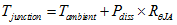
where Tambient is the ambient temperature, Pdiss is the total power dissipation, and RθJA is the thermal resistance from junction to ambient.
The total power dissipation may vary depending on the application of the DLPA3005. The main contributors in the DLPA3005 are typically:
- Buck converters
- LDOs
For the buck converter, the power dissipation is given by:
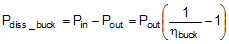
where ηbuck is the efficiency of the buck converter, Pin is the power delivered to the input of the buck converter, and Pout is the power delivered to the load of the buck converter. For the buck converter PWR1,2,6, the efficiency can be determined using the curves in Figure 7-16.
For the LDO, the power dissipation is given by:

where Vin is the input supply voltage, Vout is the output voltage of the LDO, and Iload is the load current of the LDO. The voltage drops over the LDO (Vin-Vout) can be relatively large; a small load current can result in significant power dissipation. For this situation, a general purpose buck converter can be a more efficient solution.
The LDO DMD provides power to the boost converter, and the boost converter provides high voltages for the DMD; that is, VBIAS, VOFS, VRST. The current load on these lines can increase up to Iload,max=10 mA. Assuming the efficiency of the boost converter, ηboost, is 80%, the maximum boost converter power dissipation, Pdiss_DMD_boost,max, can be calculated as:
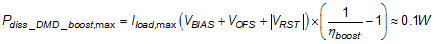
Compared to the power dissipation of the illumination buck converter, the power dissipation of the boost converter is negligible. However, the power dissipation of the LDO DMD, Pdiss_LDO_DMD should be given consideration in the case of a high supply voltage. The worst-case load current for the LDO is given by:
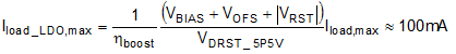
where the output voltage of the LDO is VDRST_5P5V= 5.5 V.
The worst-case power dissipation of the LDO DMD is approximately 1.5 W when the input supply voltage is 19.5 V. For your specific application, it is recommended to check the LDO current level. Therefore, the total power dissipation of the DLPA3005 can be described as:

The following examples calculate of the maximum ambient temperature and the junction temperature based on known information.
If it is assumed that the total dissipation Pdiss_DLPA3005= 2.5 W, Tjunction,max= 120°C, and RθJA= 7°C/W (refer to Section 6.4), then the maximum ambient temperature can be calculated using Equation 13:

If the total power dissipation and the ambient temperature are known as:
the junction temperature can be calculated:

If the combination of ambient temperature and the total power dissipation of the DLPA3005 does not produce an acceptable junction temperature, that is, <120°C, there are two approaches:
- Use larger heat sink or more airflow to reduced RθJA.
- Reduce power dissipation in
DLPA3005:
- Use an external buck converter instead of an internal general purpose buck converter.
- Reduce load current for the buck converter.