DLPS132 May   2018 DLPA4000

PRODUCTION DATA.  

  1. Features
  2. Applications
  3. Description
    1.     Device Images
      1.      System Block Diagram
  4. Revision History
  5. Pin Configuration and Functions
    1.     Pin Functions
  6. Specifications
    1. 6.1 Absolute Maximum Ratings
    2. 6.2 ESD Ratings
    3. 6.3 Recommended Operating Conditions
    4. 6.4 Thermal Information
    5. 6.5 Electrical Characteristics
    6. 6.6 SPI Timing Parameters
  7. Detailed Description
    1. 7.1 Overview
    2. 7.2 Functional Block Description
    3. 7.3 Feature Description
      1. 7.3.1 Supply and Monitoring
        1. 7.3.1.1 Supply
        2. 7.3.1.2 Monitoring
          1. 7.3.1.2.1 Block Faults
          2. 7.3.1.2.2 Low Battery and UVLO
          3. 7.3.1.2.3 Thermal Protection
      2. 7.3.2 Illumination
        1. 7.3.2.1 Programmable Gain Block
        2. 7.3.2.2 LDO Illumination
        3. 7.3.2.3 Illumination Driver A
        4. 7.3.2.4 External MOSFETs
          1. 7.3.2.4.1 Gate series resistor (RG)
          2. 7.3.2.4.2 Gate series diode (DG)
          3. 7.3.2.4.3 Gate parallel capacitance (CG)
        5. 7.3.2.5 RGB Strobe Decoder
          1. 7.3.2.5.1 Break Before Make (BBM)
          2. 7.3.2.5.2 Openloop Voltage
          3. 7.3.2.5.3 Transient Current Limit
        6. 7.3.2.6 Illumination Monitoring
          1. 7.3.2.6.1 Power Good
          2. 7.3.2.6.2 RatioMetric Overvoltage Protection
      3. 7.3.3 External Power MOSFET Selection
        1. 7.3.3.1 Threshold Voltage
        2. 7.3.3.2 Gate Charge and Gate Timing
        3. 7.3.3.3 On-resistance RDS(on)
      4. 7.3.4 DMD Supplies
        1. 7.3.4.1 LDO DMD
        2. 7.3.4.2 DMD HV Regulator
        3. 7.3.4.3 DMD/DLPC Buck Converters
        4. 7.3.4.4 DMD Monitoring
          1. 7.3.4.4.1 Power Good
          2. 7.3.4.4.2 Overvoltage Fault
      5. 7.3.5 Buck Converters
        1. 7.3.5.1 LDO Bucks
        2. 7.3.5.2 General Purpose Buck Converters
        3. 7.3.5.3 Buck Converter Monitoring
          1. 7.3.5.3.1 Power Good
          2. 7.3.5.3.2 Overvoltage Fault
      6. 7.3.6 Auxiliary LDOs
      7. 7.3.7 Measurement System
    4. 7.4 Device Functional Modes
    5. 7.5 Programming
      1. 7.5.1 SPI
      2. 7.5.2 Interrupt
      3. 7.5.3 Fast-Shutdown in Case of Fault
      4. 7.5.4 Protected Registers
      5. 7.5.5 Writing to EEPROM
    6. 7.6 Register Maps
  8. Application and Implementation
    1. 8.1 Application Information
    2. 8.2 Typical Application
      1. 8.2.1 Design Requirements
      2. 8.2.2 Detailed Design Procedure
        1. 8.2.2.1 Component Selection for General-Purpose Buck Converters
    3. 8.3 System Example With DLPA4000 Internal Block Diagram
  9. Power Supply Recommendations
    1. 9.1 Power-Up and Power-Down Timing
  10. 10Layout
    1. 10.1 Layout Guidelines
      1. 10.1.1 LED Driver
        1. 10.1.1.1 PowerBlock Gate Control Isolation
        2. 10.1.1.2 VIN to PowerBlocks
        3. 10.1.1.3 Return Current from LEDs and RSense
        4. 10.1.1.4 RC Snubber
        5. 10.1.1.5 Capacitor Choice
      2. 10.1.2 General Purpose Buck 2
      3. 10.1.3 SPI Connections
      4. 10.1.4 RLIM Routing
      5. 10.1.5 LED Connection
    2. 10.2 Layout Example
    3. 10.3 Thermal Considerations
  11. 11Device and Documentation Support
    1. 11.1 Device Support
      1. 11.1.1 Device Nomenclature
    2. 11.2 Receiving Notification of Documentation Updates
    3. 11.3 Community Resources
    4. 11.4 Trademarks
    5. 11.5 Electrostatic Discharge Caution
    6. 11.6 Glossary
  12. 12Mechanical, Packaging, and Orderable Information
    1. 12.1 Package Option Addendum
      1. 12.1.1 Packaging Information

Package Options

Mechanical Data (Package|Pins)
Thermal pad, mechanical data (Package|Pins)
Orderable Information

DMD Supplies

Figure 13 shows the supplies needed for the DMD and DLPC block.

  • LDO_DMD: for internal supply
  • DMD_HV: regulator generates high voltage supplies
  • Two buck converters: for DLPC/DMD voltages
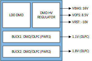
DLPA4000 DMD_System_Diagram.gifFigure 13. DMD Supplies Blocks

The DMD supplies block operates with the 0.65 DLP650NE DMD and the related DLPC4422. In addition to the three high voltage supplies to power the DLPA4000, the DMD and the related DLPC4422 each require a supply, Two buck converters provide the power.

The EEPROM of the DLPA4000 is factory programmed for a certain configuration, such as the type of buck converter used. Use register 0x26 to read the EEPROM configuration using these bits:

  • DMD_BUCK1_USE
  • DMD_BUCK2_USE

Table 8 describes the function of register 0x26.