DLPS132 May 2018 DLPA4000
PRODUCTION DATA.
- 1 Features
- 2 Applications
- 3 Description
- 4 Revision History
- 5 Pin Configuration and Functions
- 6 Specifications
-
7 Detailed Description
- 7.1 Overview
- 7.2 Functional Block Description
- 7.3
Feature Description
- 7.3.1 Supply and Monitoring
- 7.3.2 Illumination
- 7.3.3 External Power MOSFET Selection
- 7.3.4 DMD Supplies
- 7.3.5 Buck Converters
- 7.3.6 Auxiliary LDOs
- 7.3.7 Measurement System
- 7.4 Device Functional Modes
- 7.5 Programming
- 7.6 Register Maps
- 8 Application and Implementation
- 9 Power Supply Recommendations
- 10Layout
- 11Device and Documentation Support
- 12Mechanical, Packaging, and Orderable Information
Package Options
Mechanical Data (Package|Pins)
- PFD|100
Thermal pad, mechanical data (Package|Pins)
- PFD|100
Orderable Information
7.3.7 Measurement System
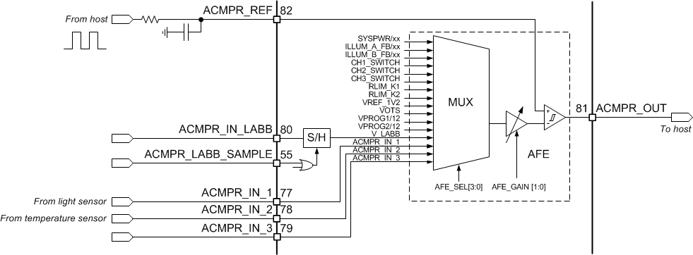
Figure 17 shows the circuitry that senses internal and external nodes. The implemented AFE comparator converts the nodes to digital signals. Use the 0x0A register to enable AFE_EN. The reference signal for this comparator, ACMPR_REF, is a low pass filtered PWM signal coming from the DLPC. A variable gain amplifier (VGA) is added with three gain settings (1x, 9.5x, and 18x) allows the device to receive a wide range of input signals . Use register 0x0A, to set the VGA gain (AFE_GAIN). The maximum input voltage of the VGA is 1.5 V. The device reduces some large internal voltage to accomodate the VGA function.
 Figure 17. Measurement System Schematic
The device connects a multiplexer (MUX) to a wide range of nodes. Use egister 0X0A, to select the MUX input (AFE_SEL) . Choose settings from these options:
- System input voltage, SYSPWR
- LED anode cathode voltage, ILLUM_A_FB
- LED cathode voltage, CHx_SWITCH
- V_RLIM to measure LED current
- Internal reference, VREF_1V2
- Die Temperature represented by voltage VOTS
- EEPROM programming voltage, VPROG1,2/12
- LABB sensor, V_LABB
- External sense pins, ACMPR_IN_1, ACMPR_IN_2, ACMPR_IN_3
The system input voltage VIN can be measured by selecting the SYSPWR/xx input of the MUX. the The device must divide the voltage before the device supplies system input voltage to the MUX. Applications require this process because the variable gain amplifier (VGA) handles voltages up-to 1.5 V but system voltages can be as high as 20 V. The device combines the division factor selection (VIN division factor) with the auto LED turn off functionality of the illumination driver . Use register 0x18 to ILLUM_LED_AUTO_OFF_SEL.
The device measures the LED voltages by monitoring the common anode of the LEDs and the cathode of each LED individually. The device senses the feedback pin of the illumination driver (ILLUM_A_FB) to measure the LED anode voltage (VLED). The device must divide the LED anode voltage before the device supplies input voltage to the MUX. The device combines the division factor with the overvoltage fault level of the illumination driver. Use register 0x19 to set VLED_OVP_VLED_RATIO. The device feeds the cathode voltages for CH1_SWITCH, CH2_SWITCH,and CH3_SWITCH directly to the MUX without a division factor.
You can determine the LED current if you know the value of the sense resistor RLIM and the voltage across the resistor. Measure the voltage at the high-side of the sense resistor can be measured by selecting MUX-input RLIM_K1. The bottom-side of the resistor connects to GND.
The VOTS pin connects to an on-chip temperature sensor. The VOTS voltage measures the device junction temperature:
The DLPA4000 has two EEPROM blocks for storage of trim bits, 0x30 to 0x35). Use these bytes for USER EEPROM also. Use MUX input VPROG1/12 to measure the programming voltage of EEPROM block 1. Use VPROGR2/12 to measure the programming voltage of EEPROM block 2. The device divides the EEPROM programming voltage by 12 and then supplies the value to the MUX to prevent a too large voltage on the MUX input. The EEPROM programming voltage is approximately 12 V.
The local area brightness boost (LABB) function increases brightness while maintaining good contrast and saturation. Connect the sensor to pin ACMPR_IN_LABB. The device samples the light sensor signal. The device holds the sample value separate from the sensor timing. Make sure the application uses these setting for LABB oepration.
- The AFE block is enabled (0x0A, AFE_EN = 1)
- The LABB input is selected (0x0A, AFE_SEL<3:0>=3h)
- The AFE gain is set appropriately to have AFE_Gain x VLABB < 1.5 V (0x0A, AFE_GAIN<1:0>)
Use one of the following methods to sample the signal.
- Write to register 0x0B by specifying the sample time window (TSAMPLE_SEL) and set bit SAMPLE_LABB=1 to start sampling. The device automatically restes the SAMPLE_LABB bit in register 0x0B to 0 at the end of the sample period to prepare for a next sample request.
- Use the input ACMPR_LABB_SAMPLE-pin as a sample signal. The signal on ACMPR_IN_LABB is tracked while it is high. After the ACMP_LABB_SAMPLE goes lowm the value the device holds the value.
ACMPR_IN_1, ACMPR_IN_2,and ACMPR_IN_3 measure external signals from components such as a light sensor or a temperature sensor. Make sure that the voltage on the input doe not exceed 1.5 V.