DLPS112C June 2018 – August 2021 DLPC3479
PRODUCTION DATA
- 1 Features
- 2 Applications
- 3 Description
- 4 Revision History
- 5 Pin Configuration and Functions
-
6 Specifications
- 6.1 Absolute Maximum Ratings
- 6.2 ESD Ratings
- 6.3 Recommended Operating Conditions
- 6.4 Thermal Information
- 6.5 Power Electrical Characteristics
- 6.6 Pin Electrical Characteristics
- 6.7 Internal Pullup and Pulldown Electrical Characteristics
- 6.8 DMD Sub-LVDS Interface Electrical Characteristics
- 6.9 DMD Low-Speed Interface Electrical Characteristics
- 6.10 System Oscillator Timing Requirements
- 6.11 Power Supply and Reset Timing Requirements
- 6.12 Parallel Interface Frame Timing Requirements
- 6.13 Parallel Interface General Timing Requirements
- 6.14 Flash Interface Timing Requirements
- 6.15 Other Timing Requirements
- 6.16 DMD Sub-LVDS Interface Switching Characteristics
- 6.17 DMD Parking Switching Characteristics
- 6.18 Chipset Component Usage Specification
-
7 Detailed Description
- 7.1 Overview
- 7.2 Functional Block Diagram
- 7.3 Feature Description
- 7.4 Device Functional Modes
- 7.5 Programming
- 8 Application and Implementation
- 9 Power Supply Recommendations
- 10Layout
- 11Device and Documentation Support
- 12Mechanical, Packaging, and Orderable Information
Package Options
Mechanical Data (Package|Pins)
- ZEZ|201
Thermal pad, mechanical data (Package|Pins)
Orderable Information
7.3.7 Local Area Brightness Boost (LABB)
Local area brightness boost (LABB), part of the IntelliBright™ suite of advanced image processing algorithms, adaptively gains up regions of an image that are dim relative to the average picture level. The controller applies significant gain to some regions of the image, and applies little or no gain to other regions. The LABB algorithm evaluates images frame-by-frame and calculates the local area gains to be used for each image. Since many images have a net overall boost in gain, even if the controller applies no gain to some parts of the image, the controller boosts the overall perceived brightness of the image.
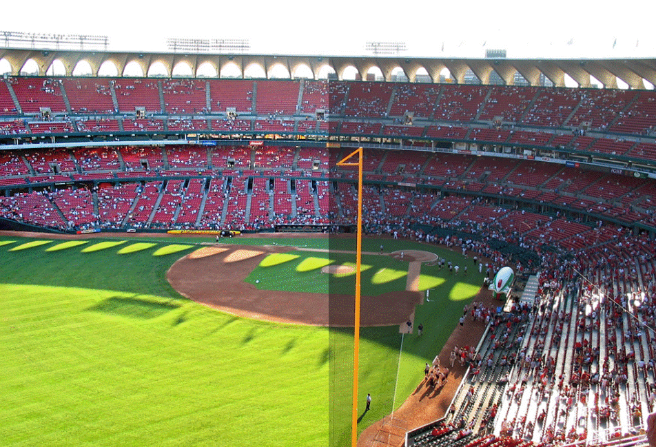
Figure 7-20 shows a split screen example of the impact of the LABB algorithm for an image that includes dark areas.
 Figure 7-20 LABB
Enabled (Left Side) and LABB Disabled (Right Side)
Figure 7-20 LABB
Enabled (Left Side) and LABB Disabled (Right Side)The LABB algorithm operates most effectively when ambient light conditions are used to help determine the decision about the strength of gains utilized. For this reason, it may be useful to include an ambient light sensor in the system design that is used to measure the display screen's reflected ambient light. This sensor can assist in dynamically controlling the LABB strength. Set the LABB gain higher for bright rooms to help overcome washed out images. Set the LABB gain lower in dark rooms to prevent overdriven pixel intensities in images.