DLPS024G August   2012  – February 2020 DLPC410

PRODUCTION DATA.  

  1. Features
  2. Applications
  3. Description
    1.     Device Images
      1.      Simplified Application
  4. Revision History
  5. Description (continued)
  6. Pin Configuration and Functions
    1.     Pin Functions
  7. Specifications
    1. 7.1 Absolute Maximum Ratings
    2. 7.2 ESD Ratings
    3. 7.3 Recommended Operating Conditions
    4. 7.4 Electrical Characteristics
    5. 7.5 Timing Requirements
  8. Detailed Description
    1. 8.1 Overview
    2. 8.2 Functional Block Diagrams
    3. 8.3 Feature Description
      1. 8.3.1 DLPC410 Binary Pattern Data Path
        1. 8.3.1.1  DIN_A, DIN_B, DIN_C, DIN_D Input Data Buses
        2. 8.3.1.2  DCLKIN Input Clocks
        3. 8.3.1.3  DVALID Input Signals
        4. 8.3.1.4  DOUT_A, DOUT_B, DOUT_C, DOUT_D Output Data Buses
        5. 8.3.1.5  DCLKOUT Output Clocks
        6. 8.3.1.6  SCTRL Output Signals
        7. 8.3.1.7  Supported DMD Bus Sizes
        8. 8.3.1.8  Row Cycle definition
        9. 8.3.1.9  DLP9500 and DLP9500UV Input Data Formatting
        10. 8.3.1.10 DLP7000 and DLP7000UV Input Data Bus
        11. 8.3.1.11 DLP650LNIR Input Data Bus
      2. 8.3.2 Data Bus Operations
        1. 8.3.2.1 Row Addressing
        2. 8.3.2.2 Single Row Write Operation
        3. 8.3.2.3 No-Op Row Cycle Description
      3. 8.3.3 DMD Block Operations
        1. 8.3.3.1 Mirror Clocking Pulse (MCP)
        2. 8.3.3.2 Reset Active (RST_ACTIVE)
        3. 8.3.3.3 DMD Block Control Signals
          1. 8.3.3.3.1 Block Mode - BLK_MD1:0)
          2. 8.3.3.3.2 Block Address - BLK_AD(3:0)
          3. 8.3.3.3.3 Reset 2 Blocks - RST2BLK
        4. 8.3.3.4 DMD Block Operations
          1. 8.3.3.4.1 Global Reset (MCP) Consideration
      4. 8.3.4 Other Data Control Inputs
        1. 8.3.4.1 Complement Data
        2. 8.3.4.2 North/South Flip
      5. 8.3.5 Miscellaneous Control Inputs
        1. 8.3.5.1 ARST
        2. 8.3.5.2 CLKIN_R
        3. 8.3.5.3 DMD_A_RESET
        4. 8.3.5.4 Watchdog Timer Enable (WDT_ENABLE)
      6. 8.3.6 Miscellaneous Status Outputs
        1. 8.3.6.1 INIT_ACTIVE
        2. 8.3.6.2 DMD_Type(3:0)
        3. 8.3.6.3 DDC_VERSION(2:0)
        4. 8.3.6.4 LED0
        5. 8.3.6.5 LED1
        6. 8.3.6.6 DLPA200 Control Signals
        7. 8.3.6.7 ECM2M_TP_ (31:0)
    4. 8.4 Device Functional Modes
      1. 8.4.1 DLPC410 Initialization and Training
        1. 8.4.1.1 Initialization
        2. 8.4.1.2 Input Data Interface (DIN) Training
      2. 8.4.2 DLPC410 Operational Modes
        1. 8.4.2.1 Single Block Mode
        2. 8.4.2.2 Single Block Phased Mode
        3. 8.4.2.3 Dual Block Mode
        4. 8.4.2.4 Quad Block Mode
        5. 8.4.2.5 Global Mode
        6. 8.4.2.6 DMD Park Mode
        7. 8.4.2.7 DMD Idle Mode
      3. 8.4.3 LOAD4 Functionality (enabled with DLPR410A)
        1. 8.4.3.1 Enabling LOAD4
        2. 8.4.3.2 Loading Data with LOAD4
        3. 8.4.3.3 Row Mapping with LOAD4
        4. 8.4.3.4 Using Block Clear with LOAD4
        5. 8.4.3.5 Timing Requirements for LOAD4
        6. 8.4.3.6 Global Binary Pattern Rate increases using LOAD4
        7. 8.4.3.7 Special LOAD4 considerations
    5. 8.5 Programming
  9. Application and Implementation
    1. 9.1 Application Information
      1. 9.1.1 Device Description
    2. 9.2 Typical Application
      1. 9.2.1 Design Requirements
      2. 9.2.2 Detailed Design Procedure
      3. 9.2.3 Application Curves
    3. 9.3 Initialization Setup
      1. 9.3.1 Debugging Guidelines
      2. 9.3.2 Initialization
        1. 9.3.2.1 Input Data Bus Calibration
        2. 9.3.2.2 DLPA200 Initialization Step 1
        3. 9.3.2.3 DMD Initialization
          1. 9.3.2.3.1 DMD Device ID Check
        4. 9.3.2.4 DLPA200 Initialization Step 2
        5. 9.3.2.5 Command Sequence Initialization
      3. 9.3.3 Image Display Issues
        1. 9.3.3.1 Present Data to DLPC410
        2. 9.3.3.2 Load Data to DMD
        3. 9.3.3.3 Mirror Clocking Pulse
  10. 10Power Supply Recommendations
    1. 10.1 Power Down Operation
  11. 11Layout
    1. 11.1 Layout Guidelines
      1. 11.1.1 Impedance Requirements
      2. 11.1.2 PCB Signal Routing
      3. 11.1.3 Fiducials
      4. 11.1.4 PCB Layout Guidelines
        1. 11.1.4.1 DMD Interface
          1. 11.1.4.1.1 Trace Length Matching
        2. 11.1.4.2 DLPC410 DMD Decoupling
          1. 11.1.4.2.1 Decoupling Capacitors
        3. 11.1.4.3 VCC and VCC2
        4. 11.1.4.4 DMD Layout
        5. 11.1.4.5 DLPA200
    2. 11.2 Layout Example
    3. 11.3 DLPC410 Chipset Connections
  12. 12Device and Documentation Support
    1. 12.1 Device Support
      1. 12.1.1 Device Marking
      2. 12.1.2 Device Nomenclature
    2. 12.2 Documentation Support
      1. 12.2.1 Related Documentation
    3. 12.3 Support Resources
    4. 12.4 Trademarks
    5. 12.5 Electrostatic Discharge Caution
    6. 12.6 Glossary
  13. 13Mechanical, Packaging, and Orderable Information

Package Options

Mechanical Data (Package|Pins)
  • DLP|676
Thermal pad, mechanical data (Package|Pins)
Orderable Information

No-Op Row Cycle Description

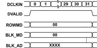
A Row No-Op is a row cycle in which setting ROW_MD = "00" commands the DLPC410 that within the current row cycle, no Row Write operation is to be performed. A Block No-Op is a row cycle in which BLK_MD = "00" commands the DLPC410 that within the current row cycle no Block Operation is to be performed. Row No-Ops can be inserted when only block operations are desired, Block No-ops can be inserted when only Row Write operations are desired, or both Row No-Ops and Block No-Ops can be performed at the same time when neither type of operation is desired (as shown in Figure 10). No-Ops are frequently inserted in the stream of data and commands when delays are desired to complete on-going operations to avoid violating delay requirements.
DLPC410 no_op_row_cyc_lps024.gifFigure 10. No-Op Row Cycle (DLP7000 example)