DLPS223A December 2021 – February 2023 DLPC4430
PRODUCTION DATA
- 1 Features
- 2 Applications
- 3 Description
- 4 Revision History
- 5 Pin Configuration and Functions
-
6 Specifications
- 6.1 Absolute Maximum Ratings
- 6.2 ESD Ratings
- 6.3 Recommended Operating Conditions
- 6.4 Thermal Information
- 6.5 Electrical Characteristics
- 6.6 System Oscillators Timing Requirements
- 6.7 Test and Reset Timing Requirements
- 6.8 JTAG Interface: I/O Boundary Scan Application Timing Requirements
- 6.9 Port 1 Input Pixel Timing Requirements
- 6.10 Port 3 Input Pixel Interface (via GPIO) Timing Requirements
- 6.11 DMD LVDS Interface Timing Requirements
- 6.12 Synchronous Serial Port (SSP) Interface Timing Requirements
- 6.13 Programmable Output Clocks Switching Characteristics
- 6.14 Synchronous Serial Port Interface (SSP) Switching Characteristics
- 6.15 JTAG Interface: I/O Boundary Scan Application Switching Characteristics
-
7 Detailed Description
- 7.1 Overview
- 7.2 Functional Block Diagram
- 7.3 Feature Description
- 7.4 Device Functional Modes
- 8 Application and Implementation
- 9 Power Supply Recommendations
- 10Layout
- 11Device and Documentation Support
- 12Mechanical, Packaging, and Orderable Information
Package Options
Mechanical Data (Package|Pins)
- ZPC|516
Thermal pad, mechanical data (Package|Pins)
Orderable Information
5 Pin Configuration and Functions
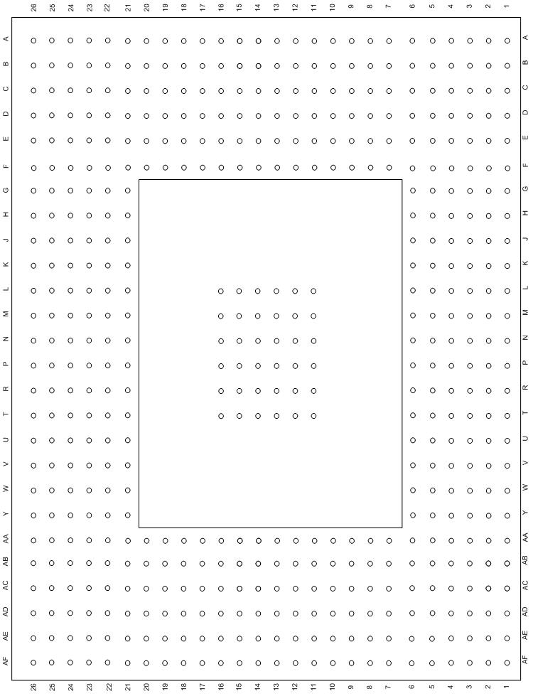
Table 5-1 Pin Functions
| PIN(1) | TYPE(2) | DESCRIPTION | ||
|---|---|---|---|---|
| NAME | NO. | |||
| POSENSE | P22 | I4 | Power-on sense, high true, signal provided from an external voltage monitor circuit. This signal is driven active (high) when all ASIC supply voltages have reached 90% of their specified minimum voltage. This signal is driven inactive (low) after the falling edge of PWRGOOD as specified. | |
| PWRGOOD | T26 | I4 | Power good, high true, signal from external power supply or voltage monitor. A high value indicates all power is within operating voltage specs and the system is safe to exit its reset state. A transition from high to low is used to indicate that the controller or DMD supply voltage drops below their rated minimum level. This transition must occur prior to the supply voltage drop as specified. During this interval, POSENSE must remain active high. This is a warning of an imminent power loss condition. This warning is required to enhance long term DMD reliability. A DMD park followed by a full controller reset is performed by the DLPC4430 controller when PWRGOOD goes low for the specified minimum, protecting the DMD. This minimum deassertion time is used to protect the input from glitches. Following this the DLPC4430 controller is held in its reset state as long as PWRGOOD is low. PWRGOOD must be driven high for normal operation. The DLPC4430 controller acknowledges PWRGOOD as active once it has been driven high for a specified minimum time. Uses hysteresis | |
| EXT_ARTZ | T24 | O2 | General purpose, low true, reset output. This output is asserted low immediately upon asserting power-up reset (POSENSE) low and remains low while POSENSE remains low. EXT_ARSTZ continues to be held low after the release of power-up reset (that is, POSENSE set high) until released by software. EXT_ARSTZ is also asserted low approximately 5 µs after the detection of a PWRGOOD or any internally generated reset. In all cases it remains active for a minimum of 2 ms. Note that the ASIC contains a software register that can be used to independently drive this output. | |
| MTR_ARTZ | T25 | O2 | Color wheel motor controller, low true, reset output. This output is asserted low immediately upon asserting power-up reset (POSENSE) low and remains low while POSENSE remains low. MTR_ARSTZ continues to be held low after the release of power-up reset (that is, POSENSE is set high) until released by software. MTR_ARSTZ is also optionally asserted low approximately 5 µs after the detection of a PWRGOOD or any internally generated reset. In all cases, it remains active for a minimum of 2 ms. Note that the ASIC contains a software register that can be used to independently drive this output. The ASIC also contains a software register that can be used to disable the assertion of motor reset upon a lamp strike reset. | |
| BOARD LEVEL TEST AND INITIALIZATION(3) | ||||
| TDI | N25 | I4 | JTAG serial data in | |
| TCK | N24 | I4 | JTAG serial data clock | |
| TMS1 | P25 | I4 | JTAG test mode select | |
| TMS2 | P26 | I4 | JTAG test mode select | |
| TDO1 | N23 | O5 | JTAG serial data out | |
| TDO2 | N22 | O5 | JTAG serial data out | |
| TRSTZ | M23 | I4 | JTAG reset. This signal includes an internal pullup and utilizes hysteresis. This pin is pulled high (or left unconnected) when the JTAG interface is in use for boundary scan or ARM debug. Connect this pin to ground otherwise. Failure to tie this pin low during normal operation causes startup and initialization problems. | |
| RTCK | E4 | O2 | JTAG return clock | |
| ETM_PIPESTAT_2 | A4 | B2 | ETM trace port pipeline status. Indicates the pipeline status of the ARM core. These signals include internal pulldowns. | |
| ETM_PIPESTAT_1 | B5 | B2 | ||
| ETM_PIPESTAT_0 | C6 | B2 | ||
| ETM_TRACESYNC | A5 | B2 | ETM trace port synchronization signal, indicating the start of a branch sequence on the trace packet port. This signal includes an internal pulldown. | |
| ETM_TRACECLK | D7 | B2 | ETM trace port clock. This signal includes an internal pulldown. | |
| ICTSEN | M24 | I4 | IC tristate enable (active high). Asserting high tristates all outputs except the JTAG interface. This signal includes an internal pulldown, however an external pulldown is recommended for added protection. Uses hysteresis. | |
| TSTPT_7 | E8 | B2 | Test pin 7. This signal provides internal pulldowns. | |
| Normal use: reserved for test output. Recommended to be left open or unconnected for normal use | ||||
| TSTPT_6 | B4 | B2 | Test pin 6. This signal provides internal pulldowns. | |
| Normal use: reserved for test output. Recommended to be left open or unconnected for normal use | ||||
| TSTPT_5 | C4 | B2 | Test pin 5. This signal provides internal pulldowns. | |
| Normal use: reserved for test output. Recommended to be left open or unconnected for normal use | ||||
| TSTPT_4 | E7 | B2 | Test pin 4. This signal provides internal pulldowns. | |
| Normal use: reserved for test output. Recommended to be left open or unconnected for normal use | ||||
| TSTPT_3 | D5 | B2 | Test pin 3. This signal provides internal pulldowns. | |
| Normal use: reserved for test output. Recommended to be left open or unconnected for normal use. | ||||
| TSTPT_2 | E6 | B2 | Test pin 2. This signal provides internal pulldowns. Additionally, it is recommended that jumper options be provided for connecting TSTPT(2:0) to external pullups. | |
| TSTPT_1 | D3 | B2 | Test pin 1. This signal provides internal pulldowns. Additionally, it is recommended that jumper options be provided for connecting TSTPT(2:0) to external pullups. | |
| TSTPT_0 | C2 | B2 | Test pin 0. This signal provides internal pulldowns. Additionally, it is recommended that jumper options be provided for connecting TSTPT(2:0) to external pullups. | |
| DEVICE TEST | ||||
| HW_TEST_EN | M25 | I4 | Device manufacturing test enable. This signal includes an internal pulldown and utilizes hysteresis. It is recommended that this signal be tied to an external ground in normal operation for added protection. | |
| PORT1 and PORT 2 CHANNEL DATA and CONTROL(4)(5)(6)(7) | ||||
| P_CLK1 | AE22 | I4 | Input Port Data Pixel Write Clock (selectable as rising or falling edge triggered, and which port it is associated with (A or B or (A and B)). This signal includes an internal pulldown. | |
| P_CLK2 | W25 | I4 | Input Port Data Pixel Write Clock (selectable as rising or falling edge triggered, and which port it is associated with (A or B or (A and B)). This signal includes an internal pulldown. | |
| P_CLK3 | AF23 | I4 | Input Port Data Pixel Write Clock (selectable as rising or falling edge triggered, and which port it is associated with (A or B or (A and B)). This signal includes an internal pulldown. | |
| P_DATAEN1 | AF22 | I4 | Active High Data Enable. Selectable as to which port it is associated with (A or B or (A and B)).This signal includes an internal pulldown. | |
| P_DATAEN2 | W24 | I4 | Active High Data Enable. Selectable as to which port it is associated with (A or B or (A and B)).This signal includes an internal pulldown. | |
| P1_A_9 | AD15 | I4 | Port 1 A Channel Input Pixel Data (bit weight 128) | |
| P1_A_8 | AE15 | I4 | Port 1 A Channel Input Pixel Data (bit weight 64) | |
| P1_A_7 | AE14 | I4 | Port 1 A Channel Input Pixel Data (bit weight 32) | |
| P1_A_6 | AE13 | I4 | Port 1 A Channel Input Pixel Data (bit weight 16) | |
| P1_A_5 | AD13 | I4 | Port 1 A Channel Input Pixel Data (bit weight 8) | |
| P1_A_4 | AC13 | I4 | Port 1 A Channel Input Pixel Data (bit weight 4) | |
| P1_A_3 | AF14 | I4 | Port 1 A Channel Input Pixel Data (bit weight 2) | |
| P1_A_2 | AF13 | I4 | Port 1 A Channel Input Pixel Data (bit weight 1) | |
| P1_A_1 | AF12 | I4 | Port 1 A Channel Input Pixel Data (bit weight 0.5) | |
| P1_A_0 | AE12 | I4 | Port 1 A Channel Input Pixel Data (bit weight 0.25) | |
| P1_B_9 | AF18 | I4 | Port 1 B Channel Input Pixel Data (bit weight 128) | |
| P1_B_8 | AB18 | I4 | Port 1 B Channel Input Pixel Data (bit weight 64) | |
| P1_B_7 | AC15 | I4 | Port 1 B Channel Input Pixel Data (bit weight 32) | |
| P1_B_6 | AC16 | I4 | Port 1 B Channel Input Pixel Data (bit weight 16) | |
| P1_B_5 | AD16 | I4 | Port 1 B Channel Input Pixel Data (bit weight 8) | |
| P1_B_4 | AE16 | I4 | Port 1 B Channel Input Pixel Data (bit weight 4) | |
| P1_B_3 | AF16 | I4 | Port 1 B Channel Input Pixel Data (bit weight 2) | |
| P1_B_2 | AF15 | I4 | Port 1 B Channel Input Pixel Data (bit weight 1) | |
| P1_B_1 | AC14 | I4 | Port 1 B Channel Input Pixel Data (bit weight 0.5) | |
| P1_B_0 | AD14 | I4 | Port 1 B Channel Input Pixel Data (bit weight 0.25) | |
| P1_C_9 | AD20 | I4 | Port 1 C Channel Input Pixel Data (bit weight 128) | |
| P1_C_8 | AE20 | I4 | Port 1 C Channel Input Pixel Data (bit weight 64) | |
| P1_C_7 | AE21 | I4 | Port 1 C Channel Input Pixel Data (bit weight 32) | |
| P1_C_6 | AF21 | I4 | Port 1 C Channel Input Pixel Data (bit weight 16) | |
| P1_C_5 | AD19 | I4 | Port 1 C Channel Input Pixel Data (bit weight 8) | |
| P1_C_4 | AE19 | I4 | Port 1 C Channel Input Pixel Data (bit weight 4) | |
| P1_C_3 | AF19 | I4 | Port 1 C Channel Input Pixel Data (bit weight 2) | |
| P1_C_2 | AF20 | I4 | Port 1 C Channel Input Pixel Data (bit weight 1) | |
| P1_C_1 | AC19 | I4 | Port 1 C Channel Input Pixel Data (bit weight 0.5) | |
| P1_C_0 | AE19 | I4 | Port 1 C Channel Input Pixel Data (bit weight 0.25) | |
| P1_VSYNC | AC20 | B2 | Port 1 Vertical Sync. This signal includes an internal pulldown. While intended to be associated with Port 1, it can be programmed for use with Port 2. | |
| P1_HSYNC | AD21 | B2 | Port 1 Horizontal Sync. This signal includes an internal pulldown. While intended to be associated with Port 1, it can be programmed for use with Port 2. | |
| P2_A_9 | AD26 | I4 | Port 2 A Channel Input Pixel Data (bit weight 128) | |
| P2_A_8 | AD25 | I4 | Port 2 A Channel Input Pixel Data (bit weight 64) | |
| P2_A_7 | AB21 | I4 | Port 2 A Channel Input Pixel Data (bit weight 32) | |
| P2_A_6 | AC22 | I4 | Port 2 A Channel Input Pixel Data (bit weight 16) | |
| P2_A_5 | AD23 | I4 | Port 1 A Channel Input Pixel Data (bit weight 8) | |
| P2_A_4 | AB20 | I4 | Port 2 A Channel Input Pixel Data (bit weight 4) | |
| P2_A_3 | AC21 | I4 | Port 2 A Channel Input Pixel Data (bit weight 2) | |
| P2_A_2 | AD22 | I4 | Port 2 A Channel Input Pixel Data (bit weight 1) | |
| P2_A_1 | AE23 | I4 | Port 2 A Channel Input Pixel Data (bit weight 0.5) | |
| P2_A_0 | AB19 | I4 | Port 2 A Channel Input Pixel Data (bit weight 0.25) | |
| P2_B_9 | Y22 | I4 | Port 2 B Channel Input Pixel Data (bit weight 128) | |
| P2_B_8 | AB26 | I4 | Port 2 B Channel Input Pixel Data (bit weight 64) | |
| P2_B_7 | AA23 | I4 | Port 2 B Channel Input Pixel Data (bit weight 32) | |
| P2_B_6 | AB25 | I4 | Port 2 B Channel Input Pixel Data (bit weight 16) | |
| P2_B_5 | AA22 | I4 | Port 2 B Channel Input Pixel Data (bit weight 8) | |
| P2_B_4 | AB24 | I4 | Port 2 B Channel Input Pixel Data (bit weight 4) | |
| P2_B_3 | AC26 | I4 | Port 2 B Channel Input Pixel Data (bit weight 2) | |
| P2_B_2 | AB23 | I4 | Port 2 B Channel Input Pixel Data (bit weight 1) | |
| P2_B_1 | AC25 | I4 | Port 2 B Channel Input Pixel Data (bit weight 0.5) | |
| P2_B_0 | AC24 | I4 | Port 2 B Channel Input Pixel Data (bit weight 0.25) | |
| P2_C_9 | W23 | I4 | Port 2 C Channel Input Pixel Data (bit weight 128) | |
| P2_C_8 | V22 | I4 | Port 2 B Channel Input Pixel Data (bit weight 64) | |
| P2_C_7 | Y26 | I4 | Port 2 C Channel Input Pixel Data (bit weight 32) | |
| P2_C_6 | Y25 | I4 | Port 2 B Channel Input Pixel Data (bit weight 16) | |
| P2_C_5 | Y24 | I4 | Port 2 C Channel Input Pixel Data (bit weight 8) | |
| P2_C_4 | Y23 | I4 | Port 2 B Channel Input Pixel Data (bit weight 4) | |
| P2_C_3 | W22 | I4 | Port 2 C Channel Input Pixel Data (bit weight 2) | |
| P2_C_2 | AA26 | I4 | Port 2 B Channel Input Pixel Data (bit weight 1) | |
| P2_C_1 | AA25 | I4 | Port 2 C Channel Input Pixel Data (bit weight 0.5) | |
| P2_C_0 | AA24 | I4 | Port 2 B Channel Input Pixel Data (bit weight 0.25) | |
| P2_VSYNC | U22 | B2 | Port 2 Vertical Sync. This signal includes an internal pulldown. While intended to be associated with Port 2, it can be programmed for use with Port 1. | |
| P2_HSYNC | W26 | B2 | Port 2 Horizontal Sync. This signal includes an internal pulldown. While intended to be associated with Port 2, it can be programmed for use with Port1. | |
| ALF INPUT PORT CONTROL | ||||
| ALF_VSYNC | AF11 | I4 | Autolock dedicated vertical sync. This signal includes an internal pulldown and uses hysteresis. | |
| ALF_HSYNC | AD11 | I4 | Autolock dedicated horizontal sync. This signal includes an internal pulldown and uses hysteresis. | |
| ALF_CSYNC | AE11 | I4 | Autolock dedicated composite sync (sync on green). This signal includes an internal pulldown and uses hysteresis. | |
| DMD RESET and BIAS CONTROL | ||||
| DADOEZ | AE7 | O5 | DAD (DLPA200 / DLPA300) Output Enable (active low) | |
| DADADDR_3 | AD6 | O5 | DAD address | |
| DADADDR_2 | AE5 | O5 | ||
| DADADDR_1 | AF4 | O5 | ||
| DADADDR_0 | AB8 | O5 | ||
| DADMODE_1 | AD7 | O5 | DAD modes | |
| DADMODE_0 | AE6 | O5 | ||
| DADSEL_1 | AE4 | O5 | DAD select | |
| DADSEL_0 | AC7 | O5 | ||
| DADSTRB | AF5 | O5 | DAD strobe | |
| DAD_INTZ | AC8 | I4 | DAD interrupt (active low). This signal typically requires an external pullup and uses hysteresis. | |
| DMD LVDS INTERFACE | ||||
| DCKA_P | V4 | O7 | DMD, LVDS I/F channel A, differential clock | |
| DCKA_N | V3 | O7 | ||
| SCA_P | V2 | O7 | DMD, LVDS I/F channel A, differential serial control | |
| SCA_N | V1 | O7 | ||
| DDA_P_15 | P4 | O7 | DMD, LVDS I/F channel A, differential serial data | |
| DDA_N_15 | P3 | O7 | DMD, LVDS I/F channel A, differential serial data | |
| DDA_P_14 | P2 | O7 | DMD, LVDS I/F channel A, differential serial data | |
| DDA_N_14 | P1 | O7 | DMD, LVDS I/F channel A, differential serial data | |
| DDA_N_12 | R1 | O7 | DMD, LVDS I/F channel A, differential serial data | |
| DDA_P_11 | T4 | O7 | DMD, LVDS I/F channel A, differential serial data | |
| DDA_N_11 | T3 | O7 | DMD, LVDS I/F channel A, differential serial data | |
| DDA_P_10 | T2 | O7 | DMD, LVDS I/F channel A, differential serial data | |
| DDA_N_10 | T1 | O7 | DMD, LVDS I/F channel A, differential serial data | |
| DDA_P_9 | U4 | O7 | DMD, LVDS I/F channel A, differential serial data | |
| DDA_N_9 | U3 | O7 | DMD, LVDS I/F channel A, differential serial data | |
| DDA_P_8 | U2 | O7 | DMD, LVDS I/F channel A, differential serial data | |
| DDA_N_8 | U1 | O7 | DMD, LVDS I/F channel A, differential serial data | |
| DDA_P_7 | W4 | O7 | DMD, LVDS I/F channel A, differential serial data | |
| DDA_N_7 | W3 | O7 | DMD, LVDS I/F channel A, differential serial data | |
| DDA_P_6 | W2 | O7 | DMD, LVDS I/F channel A, differential serial data | |
| DDA_N_6 | W1 | O7 | DMD, LVDS I/F channel A, differential serial data | |
| DDA_P_5 | Y2 | O7 | DMD, LVDS I/F channel A, differential serial data | |
| DDA_N_5 | Y1 | O7 | DMD, LVDS I/F channel A, differential serial data | |
| DDA_P_4 | Y4 | O7 | DMD, LVDS I/F channel A, differential serial data | |
| DDA_N_4 | Y3 | O7 | DMD, LVDS I/F channel A, differential serial data | |
| DDA_P_3 | AA2 | O7 | DMD, LVDS I/F channel A, differential serial data | |
| DDA_N_3 | AA1 | O7 | DMD, LVDS I/F channel A, differential serial data | |
| DDA_P_2 | AA4 | O7 | DMD, LVDS I/F channel A, differential serial data | |
| DDA_N_2 | AA3 | O7 | DMD, LVDS I/F channel A, differential serial data | |
| DDA_P_1 | AB2 | O7 | DMD, LVDS I/F channel A, differential serial data | |
| DDA_N_1 | AB1 | O7 | DMD, LVDS I/F channel A, differential serial data | |
| DDA_P_0 | AC2 | O7 | DMD, LVDS I/F channel A, differential serial data | |
| DDA_N_0 | AC1 | O7 | DMD, LVDS I/F channel A, differential serial data | |
| DCKB_P | J3 | O7 | DMD, LVDS I/F channel A, differential clock | |
| DCKB_N | J4 | O7 | DMD, LVDS I/F channel A, differential clock | |
| SCB_P | J1 | O7 | DMD, LVDS I/F channel A, differential serial control | |
| SCB_N | J2 | O7 | DMD, LVDS I/F channel A, differential serial control | |
| DDB_P_15 | N1 | O7 | DMD, LVDS I/F channel B, differential serial data | |
| DDB_N_15 | N2 | O7 | DMD, LVDS I/F channel B, differential serial data | |
| DDB_P_14 | N3 | O7 | DMD, LVDS I/F channel B, differential serial data | |
| DDB_N_14 | N4 | O7 | DMD, LVDS I/F channel B, differential serial data | |
| DDB_P_13 | M2 | O7 | DMD, LVDS I/F channel B, differential serial data | |
| DDB_N_13 | M1 | O7 | DMD, LVDS I/F channel B, differential serial data | |
| DDB_P_12 | M3 | O7 | DMD, LVDS I/F channel B, differential serial data | |
| DDB_N_12 | M4 | O7 | DMD, LVDS I/F channel B, differential serial data | |
| DDB_P_11 | L1 | O7 | DMD, LVDS I/F channel B, differential serial data | |
| DDB_N_11 | L2 | O7 | DMD, LVDS I/F channel B, differential serial data | |
| DDB_P_10 | L3 | O7 | DMD, LVDS I/F channel B, differential serial data | |
| DDB_N_10 | L4 | O7 | DMD, LVDS I/F channel B, differential serial data | |
| DDB_P_9 | K1 | O7 | DMD, LVDS I/F channel B, differential serial data | |
| DDB_N_9 | K2 | O7 | DMD, LVDS I/F channel B, differential serial data | |
| DDB_P_8 | K3 | O7 | DMD, LVDS I/F channel B, differential serial data | |
| DDB_N_8 | K4 | O7 | DMD, LVDS I/F channel B, differential serial data | |
| DDB_P_7 | H1 | O7 | DMD, LVDS I/F channel B, differential serial data | |
| DDB_N_7 | H2 | O7 | DMD, LVDS I/F channel B, differential serial data | |
| DDB_P_6 | H3 | O7 | DMD, LVDS I/F channel B, differential serial data | |
| DDB_N_6 | H4 | O7 | DMD, LVDS I/F channel B, differential serial data | |
| DDB_P_5 | G1 | O7 | DMD, LVDS I/F channel B, differential serial data | |
| DDB_N_5 | G2 | O7 | DMD, LVDS I/F channel B, differential serial data | |
| DDB_P_4 | G3 | O7 | DMD, LVDS I/F channel B, differential serial data | |
| DDB_N_4 | G4 | O7 | DMD, LVDS I/F channel B, differential serial data | |
| DDB_P_3 | F1 | O7 | DMD, LVDS I/F channel B, differential serial data | |
| DDB_N_3 | F2 | O7 | DMD, LVDS I/F channel B, differential serial data | |
| DDB_P_2 | F3 | O7 | DMD, LVDS I/F channel B, differential serial data | |
| DDB_N_2 | F4 | O7 | DMD, LVDS I/F channel B, differential serial data | |
| DDB_P_1 | E1 | O7 | DMD, LVDS I/F channel B, differential serial data | |
| DDB_N_1 | E2 | O7 | DMD, LVDS I/F channel B, differential serial data | |
| DDB_P_0 | D1 | O7 | DMD, LVDS I/F channel B, differential serial data | |
| DDB_N_0 | D2 | O7 | DMD, LVDS I/F channel B, differential serial data | |
| PROGRAM MEMORY (Flash and SRAM) INTERFACE | ||||
| PM_CSZ_0 | D13 | O5 | Input Bus D Data bit 3.
100-Ω internal LVDS termination |
|
| PM_CSZ_1 | E12 | O5 | ||
| PM_CSZ_2 | A13 | O5 | Input Bus D Data bit 5.
100-Ω internal LVDS termination |
|
| PM_ADDR_22 (GPIO 36) | A12 | B5 | ||
| PM_ADDR_21 (GPIO 35) | E11 | B5 | Input Bus D Data bit 10.
100-Ω internal LVDS termination |
|
| PM_ADDR_20 | D12 | O5 | ||
| PM_ADDR_19 | C12 | O5 | Input Bus D Data bit 11.
100-Ω internal LVDS termination |
|
| PM_ADDR_18 | B11 | O5 | ||
| PM_ADDR_17 | A11 | O5 | Input Bus D
Data bit 12. 100-Ω internal LVDS termination |
|
| PM_ADDR_16 | D11 | O5 | ||
| PM_ADDR_15 | C11 | O5 | Input Bus D
Data bit 13. 100-Ω internal LVDS termination |
|
| PM_ADDR_14 | E10 | O5 | ||
| PM_ADDR_13 | D10 | O5 | Input Bus D
Data bit 14. 100-Ω internal LVDS termination |
|
| PM_ADDR_12 | C10 | O5 | ||
| PM_ADDR_11 | B9 | O5 | Input Bus D
Data bit 15. 100-Ω internal LVDS termination |
|
| PM_ADDR_10 | A9 | O5 | ||
| PM_ADDR_9 | E9 | O5 | Output Bus A Data bit 0 to DMD | |
| PM_ADDR_8 | D9 | O5 | ||
| PM_ADDR_7 | C9 | O5 | Output Bus A Data bit 1 to DMD | |
| PM_ADDR_6 | B8 | O5 | ||
| PM_ADDR_5 | A8 | O5 | Output Bus A Data bit 2 to DMD | |
| PM_ADDR_4 | D8 | O5 | ||
| PM_ADDR_3 | C8 | O5 | Output Bus A Data bit 3 to DMD | |
| PM_ADDR_2 | B7 | O5 | ||
| PM_ADDR_1 | A7 | O5 | Output Bus A Data bit 4 to DMD | |
| PM_ADDR_0 | C7 | O5 | ||
| PM_WEZ | B12 | O5 | Output Bus A Data bit 5 to DMD | |
| PM_OEZ | C13 | O5 | ||
| PM_BLSZ_1 | B6 | O5 | Output Bus A Data bit 6 to DMD | |
| PM_BLSZ_0 | A6 | O5 | ||
| PM_DATA_15 | C17 | B5 | Output Bus A Data bit 7 to DMD | |
| PM_DATA_14 | B16 | B5 | ||
| PM_DATA_13 | A16 | B5 | Output Bus A Data bit 8 to DMD | |
| PM_DATA_12 | A15 | B5 | ||
| PM_DATA_11 | B15 | B5 | Output Bus A Data bit 9 to DMD | |
| PM_DATA_10 | D16 | B5 | ||
| PM_DATA_9 | C16 | B5 | Output Bus A Data bit 10 to DMD | |
| PM_DATA_8 | E14 | B5 | ||
| PM_DATA_7 | D15 | B5 | Output Bus A Data bit 11 to DMD | |
| PM_DATA_6 | C15 | B5 | ||
| PM_DATA_5 | B14 | B5 | Output Bus A Data bit 12 to DMD | |
| PM_DATA_4 | A14 | B5 | ||
| PM_DATA_3 | E13 | B5 | Output Bus A Data bit 13 to DMD | |
| PM_DATA_2 | D14 | B5 | ||
| PM_DATA_1 | C14 | B5 | Output Bus A Data bit 14 to DMD | |
| PM_DATA_0 | B13 | B5 | ||
| PERIPHERAL INTERFACE | ||||
| IIC0_SCL | A10 | B8 | I2C Bus 0, Clock. This bus support 400 kHz, fast mode operation. This signal requires an external pullup to 3.3 V. The minimum acceptable pullup value is 1 kΩ. This input is not 5-V tolerant. | |
| IIC0_SDA | B10 | B8 | 2C Bus 0, Data. This bus support 400 kHz, fast mode operation. This signal requires an external pullup to 3.3 V. The minimum acceptable pullup value is 1 kΩ. This input is not 5-V tolerant. | |
| SSP0_CLK | AD4 | B5 | Synchronous Serial Port 0, clock | |
| SSP0_RXD | AD5 | I4 | Synchronous Serial Port 0, receive data in | |
| SSP0_TXD | AB7 | O5 | Synchronous Serial Port 0, transmit data out | |
| SSP0_CSZ_0 | AC5 | B5 | Synchronous Serial Port 0, chip select 0 (active low) | |
| SSP0_CSZ_1 | AB6 | B5 | Synchronous Serial Port 0, chip select 1 (active low) | |
| SSP0_CSZ_2 | AC3 | B5 | Synchronous Serial Port 0, chip select 2 (active low) | |
| UART0_TXD | AB3 | O5 | UART0 transmit data output | |
| UART0_RXD | AD1 | O5 | UART0 receive data input | |
| UART0_RTSZ | AD2 | O5 | UART0 ready to send hardware flow control output (active low) | |
| UART0_CTSZ | AE2 | I4 | UART0 clear to send hardware flow control input (active low) | |
| USB_DAT_N | C5 | B9 | USB D- I/O | |
| USB_DAT_P | D6 | B9 | USB D+ I/O | |
| PMD_INTZ | AE8 | I4 | Interrupt from DLPA100 (active low). This signal requires an external pullup. Uses hysteresis | |
| CW_PWM | AD8 | O5 | Color wheel control PWM output | |
| CW_INDEX | AF7 | O5 | Color wheel index. Uses hysteresis | |
| GENERAL PURPOSE I/O (GPIO)(8) | ALTERNATE FUNCTION 1 | ALTERNATE FUNCTION 2 | ||
| GPIO_82 | E3 | B5 | N/A | N/A |
| GPIO_81 | AB10 | B2 | Reserved | N/A |
| GPIO_80 | AD9 | B2 | IR_ENABLE (O) | N/A |
| GPIO_79 | AE9 | B2 | Reserved | N/A |
| GPIO_78 | AF9 | B2 | FIELD_3D_LR (I) | N/A |
| GPIO_77 | AB11 | B2 | SAS_INTGTR_EN (O) | SENSE_PWM_OUT (O) |
| GPIO_76 | AC10 | B2 | SAS_CSZ (O) | N/A |
| GPIO_75 | AD10 | B2 | SAS_DO (O) | SENSE_FREQ_IN (I) |
| GPIO_74 | AE10 | B2 | SAS_DI (I) | SENSE_COMP_IN (I) |
| GPIO_73 | AF10 | B2 | SAS_CLK (O) | N/A |
| GPIO_72 | K24 | B2 | SSP2_DI (I) | N/A |
| GPIO_71 | K23 | B2 | SSP2_CLK (B) | N/A |
| GPIO_70 | K22 | B2 | SSP2_CSZ_1 (B) | N/A |
| GPIO_69 | J26 | B2 | SSP2_CSZ_0 (B) | N/A |
| GPIO_68 | J25 | B2 | SSP2_DO (O) | N/A |
| GPIO_67 | J24 | B2 | SP_Data_7 (O) | SSP2_CSZ_2 (B) |
| GPIO_66 | J23 | B2 | SP_Data_6 (O) | SSP0_CSZ_5 (B) |
| GPIO_65 | J22 | B2 | SP_Data_5 (O) | N/A |
| GPIO_64 | H26 | B2 | SP_Data_4 (O) | CW_PWM_2 (O) |
| GPIO_63 | H25 | B2 | SP_Data_3 (O) | CW_INDEX_2 (I) |
| GPIO_62 | H24 | B2 | SP_Data_2 (O) | SP_VC_FDBK (I) |
| GPIO_61 | H23 | B2 | SP_Data_1 (O) | N/A |
| GPIO_60 | H22 | B2 | SP_Data_0 (O) | N/A |
| GPIO_59 | G26 | B2 | SP_WG_CLK (O) | N/A |
| GPIO_58 | G25 | B2 | LED_SENSE_PULSE (O) | N/A |
| GPIO_57 | F25 | B2 | Reserved | N/A |
| GPIO_56 | G24 | B2 | UART2_RXD (O) | N/A |
| GPIO_55 | G23 | B2 | UART2_TXD (O) | N/A |
| GPIO_54 | F26 | B2 | PROG_AUX_7 (O) | N/A |
| GPIO_53 | E26 | B2 | PROG_AUX_6 (O) | N/A |
| GPIO_52 | AB12 | B2 | CSP_Data (O) | ALF_CLAMP (O) |
| GPIO_51 | AC11 | B2 | CSP_CLK (O) | ALF_COAST (O) |
| GPIO_50 | V23 | B2 | Reserved | HBT_CLKOUT (O) |
| GPIO_49 | V24 | B2 | Reserved | HBT_DO (O) |
| GPIO_48 | V25 | B2 | Reserved | HBT_CLKIN_2 (I) |
| GPIO_47 | V26 | B2 | Reserved | HBT_DI_2 (I) |
| GPIO_46 | T22 | B2 | Reserved | HBT_CLKIN_1 (I) |
| GPIO_45 | U23 | B2 | Reserved | HBT_DI_1 (I) |
| GPIO_44 | U24 | B2 | Reserved | HBT_CLKIN_0 (I) |
| GPIO_43 | U25 | B2 | Reserved | HBT_DI_0 (I) |
| GPIO_42 | U26 | B2 | Reserved | SSP0_CSZ4 (B) |
| GPIO_41 | R22 | B2 | Reserved | DASYNC (I) |
| GPIO_40 | T23 | B2 | Reserved | FSD12 (O) |
| GPIO_39 | F24 | B2 | SW reserved (Boot Hold) | SW reserved (Boot Hold) |
| GPIO_38 | E25 | B2 | SW reserved (USB Enumeration Enable) | SW reserved (USB Enumeration Enable) |
| GPIO_37 | G22 | B2 | N/A | N/A |
| GPIO_36 | A12 | B2 | PM_ADDR_22 (O) | I2C_2 SDA (B) |
| GPIO_35 | E11 | B2 | PM_ADDR_21 (O) | I2C_2 SCL (B) |
| GPIO_34 | F23 | B2 | SSP1_CSZ_1 (B) | N/A |
| GPIO_33 | D26 | B2 | SSP1_CSZ_0 (B) | N/A |
| GPIO_32 | E24 | B2 | SSP1_DO (O) | N/A |
| GPIO_31 | F22 | B2 | SSP1_DI (I) | N/A |
| GPIO_30 | D25 | B2 | SSP1_CLK (B) | N/A |
| GPIO_29 | E23 | B2 | IR1 (I) | SSP2 BC CSZ (B) |
| GPIO_28 | C26 | B2 | IR0 (I) | SSP2 BC CSZ (B) |
| GPIO_27 | AB4 | B2 | SSP0_CSZ3 (B) | N/A |
| GPIO_26 | D24 | B2 | Blue LED enable (O) | UART2 TXD (O) |
| GPIO_25 | C25 | B2 | Green LED enable (O) | LAMPSYNC (O) |
| GPIO_24 | B26 | B2 | Red LED enable (O) | N/A |
| GPIO_23 | E21 | B2 | LED Dual Current Control (O) | N/A |
| GPIO_22 | D22 | B2 | LED Dual Current Control (O) | N/A |
| GPIO_21 | E20 | B2 | LED Dual Current Control (O) | N/A |
| GPIO_20 | C23 | B2 | N/A | N/A |
| GPIO_19 | D21 | B2 | N/A | N/A |
| GPIO_18 | B24 | B2 | N/A | N/A |
| GPIO_17 | C22 | B2 | General Purpose Clock 2 (O) | N/A |
| GPIO_16 | B23 | B2 | General Purpose Clock 1 (O) | N/A |
| GPIO_15 | E19 | B2 | I2C_1 SDA (B) | N/A |
| GPIO_14 | D20 | B2 | I2C_1 SCL (B) | N/A |
| GPIO_13 | C21 | B2 | PWM IN_1 (I) | I2C_2 SDA (B) |
| GPIO_12 | B22 | B2 | PWM IN_0 (I) | I2C_2 SCL (B) |
| GPIO_11 | A23 | B2 | PWM STD_7 (O) | N/A |
| GPIO_10 | A22 | B2 | PWM STD_6 (O) | N/A |
| GPIO_9 | B21 | B2 | PWM STD_5 (O) | N/A |
| GPIO_8 | A21 | B2 | PWM STD_4 (O) | N/A |
| GPIO_7 | A20 | B2 | PWM STD_3 (O) | N/A |
| GPIO_6 | C20 | B2 | PWM STD_2 (O) | N/A |
| GPIO_5 | B20 | B2 | PWM STD_1 (O) | N/A |
| GPIO_4 | B19 | B2 | PWM STD_0 (O) | N/A |
| GPIO_3 | A19 | B2 | UART1_RTSZ (O) | N/A |
| GPIO_2 | E18 | B2 | UART1_CTSZ (I) | N/A |
| GPIO_1 | D19 | B2 | UART1_RXD (I) | N/A |
| GPIO_0 | C19 | B2 | UART1_TXD (O) | N/A |
| CLOCK and PLL SUPPORT | ||||
| MOSC | M26 | I10 | System clock oscillator input (3.3-V LVTTL). Note that MOSC must be stable a maximum of 25 ms after POSENSE transitions from low to high. | |
| MOSCN | N26 | O10 | MOSC crystal return | |
| OCLKA | AF6 | O5 | General purpose output clock A. Targeted for driving the CW motor controller. The frequency is software programmable. Power-up default 787 KHz. Note that the output frequency is not affected by non-power-up reset operations (it will hold the last value programmed). | |
| DUAL CONTROLLER SUPPORT | ||||
| SEQ_SYNC | AB9 | B3 | Sequence sync. This signal is used in multi-controller configurations only, in which case the SEQSYNC signal from each controller is connected together with an external pullup. This signal is either pulled high or pulled low and not allowed to float for single controller configurations. | |
| POWER and GROUND | ||||
| VDD33 | F20, F17, F11, F8, L21, R21, Y21, AA19, AA16, AA10, AA7 | POWER | 3.3-V I/O power | |
| VDD18 | C1, F5, G6, K6, M5, P5, T5, W6, AA5, AE1, H5, N6, T6, AA13, U21, P21, H21, F14 | POWER | 1.8-V internal DRAM and LVDS I/O power | |
| VDD11 | F19, F16, F13, F10, F7, H6, L6, P6, U6, Y6, AA8, AA11, AA14, AA17, AA20, W21, T21, N21, K21, G21, L11, T11, T16, L16 | POWER | 1.15-V core power | |
| VDD_PLLD | L22 | POWER | 1.15-V DMD clock generator PLL digital power | |
| VSS_PLLD | L23 | GROUND | 1.15-V DMD clock generator PLL digital ground | |
| VAD_PLLD | K25 | POWER | 1.8-V DMD clock generator PLL analog power | |
| VAS_PLLD | K26 | GROUND | 1.8-V DMD clock generator PLL analog ground | |
| VDD_PLLM1 | L26 | POWER | 1.15-V master-LS clock generator PLL digital power | |
| VSS_PLLM1 | M22 | GROUND | 1.15-V master-LS clock generator PLL digital ground | |
| VAD_PLLM1 | L24 | POWER | 1.8-V master-LS clock generator PLL analog power | |
| VAS_PLLM1 | L25 | GROUND | 1.8-V master-LS clock generator PLL analog ground | |
| VDD_PLLM2 | P23 | POWER | master-HS clock generator PLL digital power | |
| VSS_PLLM2 | P24 | GROUND | master-HS clock generator PLL digital ground | |
| VAD_PLLM2 | R25 | POWER | 1.8-V master-HS clock generator PLL analog power | |
| VAS_PLLM2 | R26 | GROUND | 1.8-V master-HS clock generator PLL analog ground | |
| VAD_PLLS | R23 | POWER | video-2X clock generator PLL analog power | |
| VAS_PLLS | R24 | GROUND | video-2X clock generator PLL analog ground | |
| L-VDQPAD_[7:0], R-VDQPAD_[7:0] | B18, D18, B17, E17, A18, C18, A17, D17, AE17, AC17, AF17, AC18, AB16, AD17, AB17, AD18 | RESERVED | These pins have to be tied directly to ground for normal operation. | |
| CFO_VDD33 | AE26 | RESERVED | This pin has to be tied directly to 3.3 I/O power (VDD33) for normal operation. | |
| VTEST1, VTEST2, VTEST3, VTEST4 | AB14, AB15, E15, E16 | RESERVED | These pins have to be tied directly to ground for normal operation. | |
| LVDS_AVS1, LVDS_AVS2 | V5, K5 | POWER | These pins have to be tied directly to ground for normal operation. | |
| VPGM | AC6 | POWER | This pin has to be tied directly to ground for normal operation. | |
| GROUND | A26, A25, A24, B25, C24, D23, E22, F21, F18, F15, F12, F9, F6, E5, D4, C3, B3, A3, B2, A2, B1, A1 G5, J5, J6, L5, M6, N5, R5, R6, U5, V6, W5, Y5, AA6, AB5, AC4, AD3, AE3, AF3, AF2, AF1, AA9, AA12, AA15, AA18, AA21, AB22, AC23, AD24, AE24, AF24, AE25, AF25, AF26, V21, M21, J21, L15, L14, L13, L12, M16, M15, M14, M13, M12, M11, N16, N15, N14, N13, N12, N11, P16, P15, P14, P13, P12, P11, R16, R15, R14, R13, R12, R11, T15, T14, T13, T12 | GROUND | Common ground | |
(1) For instructions on handling unused pins, see General
Handling Guidelines for Unused CMOS-Type Pins.
(2) I/O Type: I = Input, O = Output, B = Bidirectional, and H =
Hysteresis. See #GUID-E6A6F879-2C12-45C4-B075-74E624579563/X5859 for subscript explanation.
(3) All JTAG signals are LVTTL compatible.
(4) Ports 1 and 2 can each be used to support multiple source
options for a given product (for example AFE and HDMI). To do so, the data bus
from both source components must be connected to the same port pins (1 or 2) and
control given to the DLPC4430 device to
tristate
the "inactive" source. Tying them together like this causes some signal
degradation due to reflections on the
tristated
path. Given the clock is the most critical signal, three Port clocks (1,
2,
and 3) are provided to provide an option to improve the signal
integrity.
(5) Ports 1 and 2 can be used separately as two 30-bit ports, or
can be combined into one 60-bit port (typically for high data rate sources) for
transmission of two pixels per clock.
(6) The A, B, C input data channels of Ports 1 and 2 can be
internally
reconfigured/
remapped
for optimum board layout.
(7) Sources feeding less than the full 10-bits per color component
channel have to be MSB justified when connected to the DLPC4430 controller and the LSBs tied off to zero. For example an
8-bit per color input has to be connected to bits 9:2 of the corresponding A, B,
C input channel.
(8) GPIO signals must be configured by software for input, output,
bidirectional, or open-drain. Some GPIOs have one or more alternate use modes,
which are also software configurable. The reset default for all optional GPIOs
is as an input signal. However, any alternate function connected to these GPIO
pins with the exception of general-purpose clocks and PWM generation, are reset.
An external pullup to the
3.3-V
supply is required for each signal configured as open-drain. External pullup or
pulldown resistors may be required to ensure stable operation before software is
able to configure these ports.
Table 5-2 I/O Type Subscript
Definition
| SUBSCRIPT | DESCRIPTION | ESD STRUCTURE |
|---|---|---|
| 2 | 3.3-V LVTTL I/O buffer with 8-mA drive | ESD diode to VDD33 and GROUND |
| 3 | 3.3-V LVTTL I/O buffer with 12-mA drive | |
| 4 | 3.3-V LVTTL receiver | |
| 5 | 3.3-V LVTTL I/O buffer with 8-mA drive, with slew rate control | |
| 6 | 3.3-V LVTTL I/O buffer, with programmable 4-mA, 8-mA, or 12-mA drive | |
| 7 | 1.8-V LVDS (DMD I/F) | |
| 8 | 3.3-V I2C with 3 mA sink | |
| 9 | USB Compatible (3.3 V) | |
| 10 | OSC 3.3-V I/O Compatible LVTTL |