DLPS031C December 2013 – August 2015 DLPC6401
PRODUCTION DATA.
- 1 Features
- 2 Applications
- 3 Description
- 4 Revision History
- 5 Pin Configuration and Functions
-
6 Specifications
- 6.1 Absolute Maximum Ratings
- 6.2 ESD Ratings
- 6.3 Recommended Operating Conditions
- 6.4 Thermal Information
- 6.5 Electrical Characteristics
- 6.6 Electrical Characteristics (Normal Mode)
- 6.7 System Oscillators Timing Requirements
- 6.8 Test and Reset Timing Requirements
- 6.9 JTAG Interface: I/O Boundary Scan Application Timing Requirements
- 6.10 Port 1 Input Pixel Interface Timing Requirements
- 6.11 Port 2 Input Pixel Interface (FPD-Link Compatible LVDS Input) Timing Requirements
- 6.12 Synchronous Serial Port (SSP) Interface Timing Requirements
- 6.13 Programmable Output Clocks Switching Characteristics
- 6.14 Synchronous Serial Port (SSP) Interface Switching Characteristics
- 6.15 JTAG Interface: I/O Boundary Scan Application Switching Characteristics
- 7 Detailed Description
- 8 Application and Implementation
- 9 Power Supply Recommendations
- 10Layout
- 11Device and Documentation Support
- 12Mechanical, Packaging, and Orderable Information
Package Options
Mechanical Data (Package|Pins)
- ZFF|419
Thermal pad, mechanical data (Package|Pins)
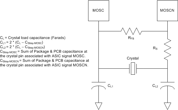
8.2.1.1 Recommended MOSC Crystal Oscillator Configuration
Table 8. Crystal Port Characteristics
| PARAMETER | NOMINAL | UNIT |
|---|---|---|
| MOSC to GND capacitance | 3.9 | pF |
| MOSCZ to GND capacitance | 3.8 | pF |
Table 9. Recommended Crystal Configuration(1)
| PARAMETER | RECOMMENDED | UNIT |
|---|---|---|
| Crystal circuit configuration | Parallel resonant | |
| Crystal type | Fundamental (first harmonic) | |
| Crystal nominal frequency | 32 | MHz |
| Crystal frequency temperature stability | ±30 | PPM |
| Overall crystal frequency tolerance (including accuracy, stability, aging, and trim sensitivity) | ±100 | PPM |
| Crystal ESR | 50 (max) | Ω |
| Crystal load | 10 | pF |
| Crystal shunt load | 7 (max) | pF |
| RS drive resistor (nominal) | 100 | Ω |
| RFB feedback resistor (nominal) | 1 | MΩ |
| CL1 external crystal load capacitor (MOSC) | See (1) | pF |
| CL2 external crystal load capacitor (MOSCN) | See (1) | pF |
| PCB layout | TI recommends a ground isolation ring around the crystal. |
(1) Typical drive level with the TCX 9C32070001 crystal (ESRmax = 30 Ω) = 160 µW
 Figure 14. Recommended Crystal Oscillator Configuration
It is assumed that the external crystal oscillator will stabilize within 50 ms after stable power is applied.