DLPS206 May 2021 DLPC7540
PRODUCTION DATA
- 1 Features
- 2 Applications
- 3 Description
- 4 Revision History
- 5 Pin Configuration and Functions
-
6 Specifications
- 6.1 Absolute Maximum Ratings
- 6.2 ESD Ratings
- 6.3 Recommended Operating Conditions
- 6.4 Thermal Information
- 6.5 Power Electrical Characteristics
- 6.6 Pin Electrical Characteristics
- 6.7 DMD HSSI Electrical Characteristics
- 6.8 DMD Low-Speed LVDS Electrical Characteristics
- 6.9 V-by-One Interface Electrical Characteristics
- 6.10 FPD-Link LVDS Electrical Characteristics
- 6.11 USB Electrical Characteristics
- 6.12 System Oscillator Timing Requirements
- 6.13 Power Supply and Reset Timing Requirements
- 6.14 DMD HSSI Timing Requirements
- 6.15 DMD Low-Speed LVDS Timing Requirements
- 6.16 V-by-One Interface General Timing Requirements
- 6.17 FPD-Link Interface General Timing Requirements
- 6.18 Source Frame Timing Requirements
- 6.19 Synchronous Serial Port Interface Timing Requirements
- 6.20 Master and Slave I2C Interface Timing Requirements
- 6.21 Programmable Output Clock Timing Requirements
- 6.22 JTAG Boundary Scan Interface Timing Requirements (Debug Only)
- 6.23 JTAG ARM Multi-Ice Interface Timing Requirements (Debug Only)
- 6.24 Multi-Trace ETM Interface Timing Requirements
- 7 Detailed Description
- 8 Application and Implementation
- 9 Power Supply Recommendations
-
10Layout
- 10.1
Layout Guidelines
- 10.1.1 General Layout Guidelines
- 10.1.2 Power Supply Layout Guidelines
- 10.1.3 Layout Guidelines for Internal Controller PLL Power
- 10.1.4 Layout Guideline for DLPC7540 Reference Clock
- 10.1.5 V-by-One Interface Layout Considerations
- 10.1.6 FPD-Link Interface Layout Considerations
- 10.1.7 USB Interface Layout Considerations
- 10.1.8 DMD Interface Layout Considerations
- 10.1.9 General Handling Guidelines for Unused CMOS-Type Pins
- 10.1.10 Maximum Pin-to-Pin, PCB Interconnects Etch Lengths
- 10.2 Thermal Considerations
- 10.1
Layout Guidelines
- 11Device and Documentation Support
- 12Mechanical, Packaging, and Orderable Information
Package Options
Mechanical Data (Package|Pins)
- ZDC|676
Thermal pad, mechanical data (Package|Pins)
Orderable Information
6.13 Power Supply and Reset Timing Requirements
| PARAMETER | MIN | MAX | UNIT | ||
|---|---|---|---|---|---|
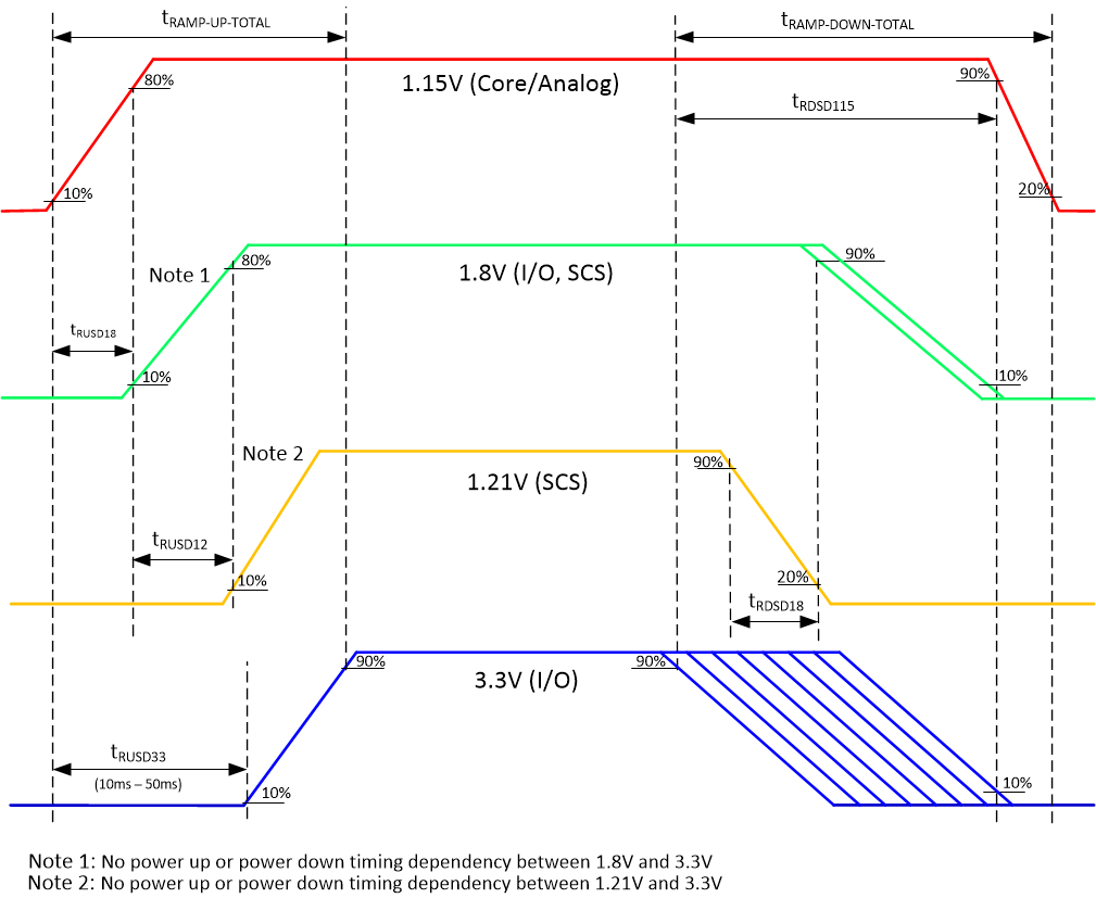
| tRAMP-UP | Power supply ramp-up time.(1) Figure 6-5 | Power supply ramp for each supply Ramp-up time: TOV × 10% to TOV × 90% TOV = Typical Operational Voltage |
0.01 | 10 | ms |
| tRAMP-UP-TOTAL | Total power supply ramp-up time.(1) | Total time within which the 1.15-V, 1.8-V, 1.21-V,
and 3.3-V supplies must complete their ramp-up from the start of the
1.15-V ramp-up. Ramp-up time: TOV × 10% to TOV × 90% TOV = Typical Operational Voltage |
100 | ms | |
| tRAMP-DOWN | Power supply ramp-down time. (1) Figure 6-5 Figure 6-6 | Power supply ramp for each supply Ramp-down time: TOV × 90% to TOV × 10% TOV = Typical Operational Voltage |
0 | 100 | ms |
| tRAMP-DOWN-TOTAL | Total power supply ramp-down time.(1) | Total time within which the 1.15-V, 1.8-V, 1.21-V,
and 3.3-V supplies must complete their ramp-down from the start of
the 3.3-V ramp-up. Ramp-down time: TOV × 90% to TOV × 10% TOV = Typical Operational Voltage |
100 | ms | |
| tRUSD18 | 1.8-V Supply Ramp-up Start Delay (2) Figure 6-6 | Delay from 1.15-V supply ramp start to 1.8-V supply ramp start. | See (3) | ms | |
| tRUSD33 | 3.3-V Supply Ramp-up Start Delay (2) Figure 6-6 | Delay from 1.15-V supply ramp start to 3.3-V supply ramp start | 10 | 50 | ms |
| tRUSD12 | 1.21-V Supply Ramp-up Start Delay (2) Figure 6-6 | Delay from 1.8-V supply ramp start to 1.21-V supply ramp start. | See (4) | ms | |
| tRDSD18 | 1.8-V Supply Ramp-down Start Delay (2) Figure 6-6 | Delay from 1.21-V supply ramp start to 1.8-V supply ramp start. | See (5) | ms | |
| tRDSD115 | 1.15-V Supply Ramp-down Start Delay (2) Figure 6-6 | Delay from 3.3-V supply ramp start to 1.15-V supply ramp start. | See(8) | ||
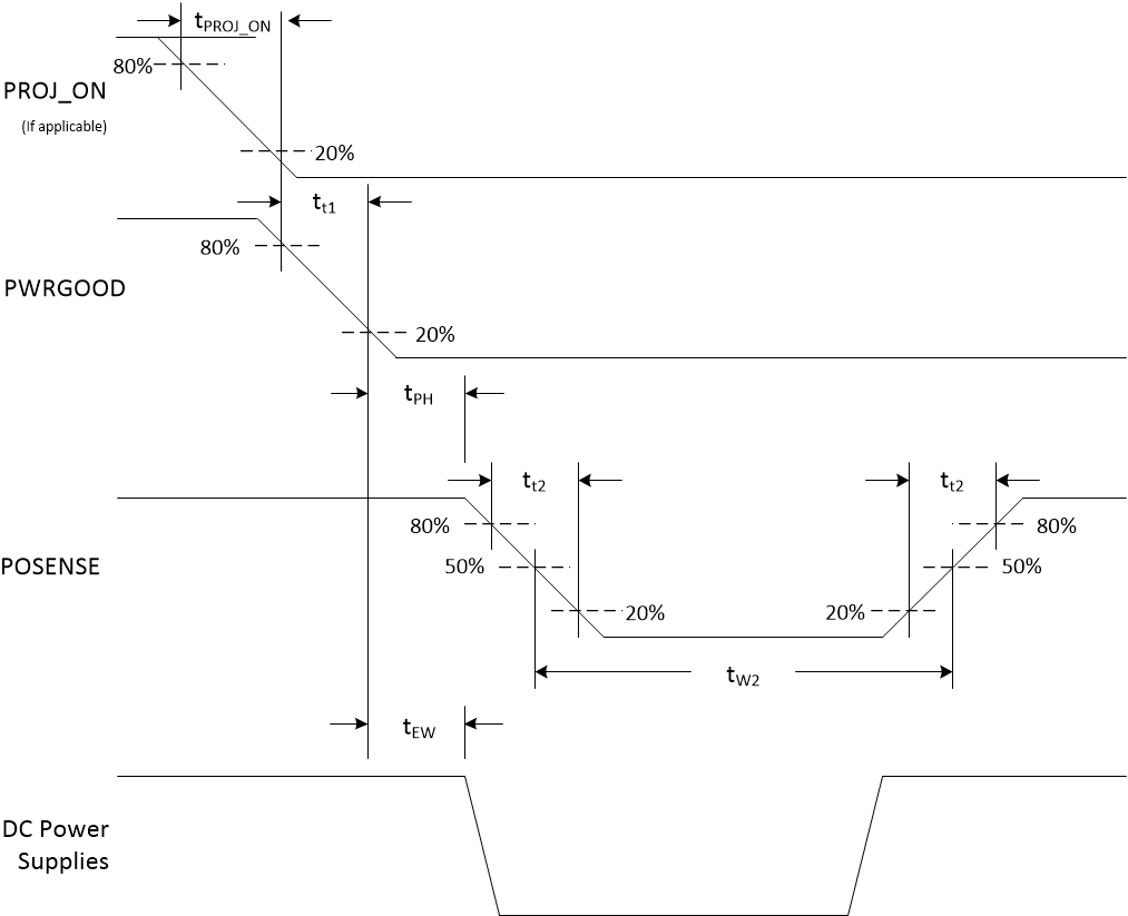
| tEW | Early Warning Time Figure 6-8 | PWRGOOD goes inactive low (as an early warning) prior to any power supply voltage going below the controller specification | 500 | µs | |
| tPH | Power Hold Time Figure 6-8 | POSENSE remains active after PWRGOOD is disabled | 500(9) | µs | |
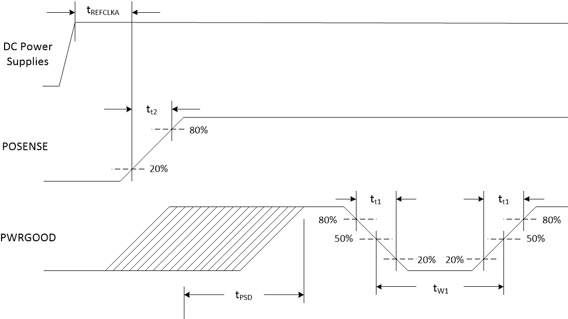
| tw1 | Pulse duration, in-active low, PWRGOOD Figure 6-7 | PWRGOOD inactive time while POSENSE is active 50% to 50% reference points (signal) |
4 | 1000 (6) | µs |
| tt1 | Transition time, PWRGOOD tt1 = tƒ1 and tr1 Figure 6-7 |
Rise and Fall time for PWRGOOD 20% to 80% reference points (signal) |
625 | µs | |
| tw2 | Pulse duration, in-active low, POSENSE Figure 6-8 | POSENCE inactive time while PWRGOOD is inactive 50% to 50% reference points (signal) |
100 | ms | |
| tt2 | Transition time, POSENSE tt1 = tƒ1 and tr1 Figure 6-8 |
Rise and Fall time for POSENSE (7) 20% to 80% reference points (signal) |
25 | µs | |
| tPSD | PWRGOOD Start Delay Figure 6-7 | Time after rising edge of POSENSE before PWRGOOD effects DLPC7540 operation | 51.5 | 60 | ms |
| tPROJ_ON | PROJ_ON fall time delay to PWRGOOD Figure 6-8 | Fall Delay PROJ_ON 80% to PWRGOOD 80% fall time start |
10 | ms | |
| tREFCLKA | Time to stable REFCLKA Figure 6-7 | Time to stable REFLCKA before POSENSE | See (10) | ||
(1) It is assumed that all 1.15-V supplies come from the same source,
although some can have additional filtering before entering the DLPC7540. As such, it is expected these supplies to ramp
together (aside from differences caused by filtering). This same expectation is
true for the 1.21-V, 1.8-V, and 3.3-V supplies.
(2) The DLPC7540 has specific power supply sequencing
requirements which are listed below, and which also include the timings
specified in this table.
- Power Up Order:
- 1.15-V (Core, Analog) » 1.8-V (I/O, SCS) » 1.21-V (SCS)
- 1.15-V (Core, Analog) » 3.3-V (I/O
- Power Down Order:
- 3.3-V (I/O) » 1.15-V (Core, Analog)
- 1.21-V (SCS) » 1.8-V (I/O, SCS) » 1.15-V (Core, Analog)
(3) This delay requirement parameter is defined as the time between two
events. The first event is the point where the 1.15-V power supply ramp-up is
started, and the second event is when the 1.15-V supply ramp-up reaches 80% of
TOV (at which point the 1.8-V supply can start its ramp-up). Because the
occurrence of the second event depends on the specific design of the 1.15-V
power supply, the designer must determine the specific delay time.
(4) This delay requirement parameter is defined as the time between two
events. The first event is the point where the 1.8-V power supply ramp-up is
started, and the second event is when the 1.8-V supply ramp-up reaches 80% of
TOV (at which point the 1.21-V supply can start its ramp-up). Because the
occurrence of the second event depends on the specific design of the 1.8-V power
supply, the designer must determine the specific delay time.
(5) This delay requirement parameter is defined as the time between two
events. The first event is the point where the 1.21-V power supply ramp-down is
started, and the second event is when the 1.21-V supply ramp-down reaches 20% of
TOV (at which point the 1.8-V supply can start its ramp-down). Because the
occurrence of the second event depends on the specific design of the 1.21-V
power supply, the designer must determine the specific delay time.
(6) This max value is only applicable if the 1.8-V power remains ON while
PWRGOOD is inactive. Otherwise, there is no maximum limit.
(7) As long as noise on this signal is below the hysteresis
threshold
(8) This delay requirement parameter
is defined as the time between two events. The first event is the point where
the 3.3-V power supply ramp-down is started, and the second event is when the
3.3-V supply ramp-down and 1.8-V supply ramp down reaches 10% of TOV (at which
point the 1.15-V supply can start its ramp-down). Because the occurrence of the
second event depends on the specific design of the 3.3V and 1.8-V power supply,
the designer must determine the specific delay time.
(9) If PROJ_ON is used for power down
then Power Hold Time (tPH) is not required.
(10) This delay requirement parameter
is defined by design of RECLKA oscillator. Stable clock must be provided before
releasing POSENSE.
 Figure 6-5 Power
Supply Ramp Time
 Figure 6-6 Power
Supply Ramp Sequencing Profiles
 Figure 6-7 Power Up
Timing
 Figure 6-8 Power
Down Timing