DLPS206 May 2021 DLPC7540
PRODUCTION DATA
- 1 Features
- 2 Applications
- 3 Description
- 4 Revision History
- 5 Pin Configuration and Functions
-
6 Specifications
- 6.1 Absolute Maximum Ratings
- 6.2 ESD Ratings
- 6.3 Recommended Operating Conditions
- 6.4 Thermal Information
- 6.5 Power Electrical Characteristics
- 6.6 Pin Electrical Characteristics
- 6.7 DMD HSSI Electrical Characteristics
- 6.8 DMD Low-Speed LVDS Electrical Characteristics
- 6.9 V-by-One Interface Electrical Characteristics
- 6.10 FPD-Link LVDS Electrical Characteristics
- 6.11 USB Electrical Characteristics
- 6.12 System Oscillator Timing Requirements
- 6.13 Power Supply and Reset Timing Requirements
- 6.14 DMD HSSI Timing Requirements
- 6.15 DMD Low-Speed LVDS Timing Requirements
- 6.16 V-by-One Interface General Timing Requirements
- 6.17 FPD-Link Interface General Timing Requirements
- 6.18 Source Frame Timing Requirements
- 6.19 Synchronous Serial Port Interface Timing Requirements
- 6.20 Master and Slave I2C Interface Timing Requirements
- 6.21 Programmable Output Clock Timing Requirements
- 6.22 JTAG Boundary Scan Interface Timing Requirements (Debug Only)
- 6.23 JTAG ARM Multi-Ice Interface Timing Requirements (Debug Only)
- 6.24 Multi-Trace ETM Interface Timing Requirements
- 7 Detailed Description
- 8 Application and Implementation
- 9 Power Supply Recommendations
-
10Layout
- 10.1
Layout Guidelines
- 10.1.1 General Layout Guidelines
- 10.1.2 Power Supply Layout Guidelines
- 10.1.3 Layout Guidelines for Internal Controller PLL Power
- 10.1.4 Layout Guideline for DLPC7540 Reference Clock
- 10.1.5 V-by-One Interface Layout Considerations
- 10.1.6 FPD-Link Interface Layout Considerations
- 10.1.7 USB Interface Layout Considerations
- 10.1.8 DMD Interface Layout Considerations
- 10.1.9 General Handling Guidelines for Unused CMOS-Type Pins
- 10.1.10 Maximum Pin-to-Pin, PCB Interconnects Etch Lengths
- 10.2 Thermal Considerations
- 10.1
Layout Guidelines
- 11Device and Documentation Support
- 12Mechanical, Packaging, and Orderable Information
Package Options
Mechanical Data (Package|Pins)
- ZDC|676
Thermal pad, mechanical data (Package|Pins)
Orderable Information
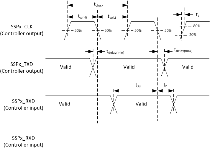
6.19 Synchronous Serial Port Interface Timing Requirements
For SSP0, SSP1 and SSP2(1)(2)
| PARAMETER | MIN | MAX | UNIT | ||
|---|---|---|---|---|---|
| SSP Master | |||||
| fclock | Clock frequency, SSPx_CLK | 50% to 50% reference points | 0.38 | 39.0 | MHz |
| tclock | Clock Period, SSPx_CLK | 50% to 50% reference points | 25.6 | 3632 | ns |
| tw(L) | Pulse duration low, SSPx_CLK | 50% to 50% reference points | 12.0 | ns | |
| tw(H) | Pulse duration high, SSPx_CLK | 50% to 50% reference points | 12.0 | ns | |
| tdelay | Output Delay – SSPx_TXD (MOSI) | -2.5 | 2.5 | ns | |
| tsu | Setup time – SSPx_RXD (MISO) | 50% to 50% reference points | 15.0 | ns | |
| th | hold time – SSPx_RXD (MISO) | 50% to 50% reference points | 0 | ns | |
| tt | Transition time (tr and tf- SSPx_RXD | 20% to 80% reference points | 1.5 | ns | |
| tclkjit | Clock Jitter, SSPx_CLK | 300 | ps | ||
| tdelay∆ | Clock output delay ∆ { | tw(H) - tw(L) | } | 500 | ps | ||
| SSP Slave | |||||
| tdelay | Output Delay – SSPx_TXD (MOSI) | 0 | 15 | ns | |
| tsu | Setup time – SSPx_RXD (MISO) | 50% to 50% reference points | 2.5 | ns | |
| th | hold time – SSPx_RXD (MISO) | 50% to 50% reference points | 2.5 | ns | |
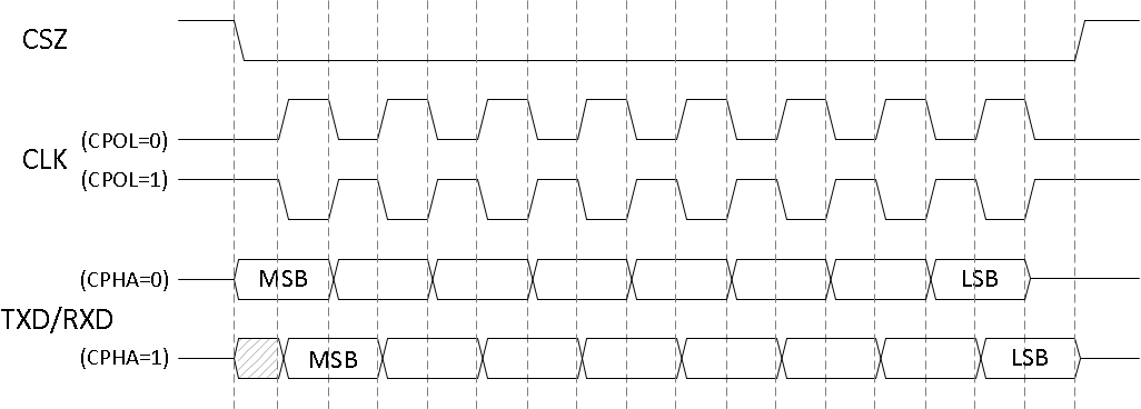
(1) The DLPC7540 SPI interfaces support SPI Modes 0, 1,
2, and 3 (that is, both clock polarities and both clock phases) as shown in
Table 6-2 and Figure 6-16. As such, each SPI interface configuration must be setup to match the SPI
mode being used.
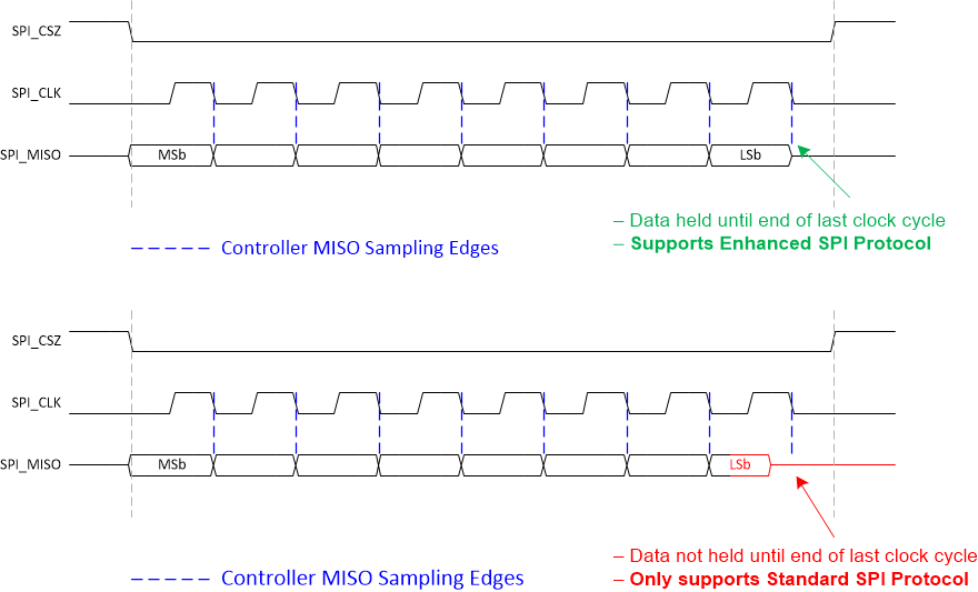
(2) In most SPI applications, one clock edge is used by both master and slave devices for
transmitting data while the other edge is use by both for sampling received
data. This is referred to as Standard SPI Protocol. To maximize the
SPI_CLK frequency potential, SPI masters can alternatively be designed to sample
the data in (MISO) bit on the same clock edge used to transmit the next data out
(MOSI) bit. This is referred to as Enhanced SPI Protocol. The DLPC7540 SPI master implementation supports both protocols (part
of SPI interface configuration), however, to be able to use the "Enhanced SPI
Protocol", the slave device must meet the requirement shown in Figure 6-17.
Table 6-2 SPI Clocking Modes
| SPI Clocking Mode | SPI Clock Polarity | SPI Clock Phase |
|---|---|---|
| 0 | 0 | 0 |
| 1 | 0 | 1 |
| 2 | 1 | 0 |
| 3 | 1 | 1 |
 Figure 6-16 Timing Diagram for SPI Clocking Modes
 Figure 6-17 Requirement for Enhanced SPI Protocol
 Figure 6-18 Timing Diagram for SSP Master (Modes 0/3)