DLPS206 May 2021 DLPC7540
PRODUCTION DATA
- 1 Features
- 2 Applications
- 3 Description
- 4 Revision History
- 5 Pin Configuration and Functions
-
6 Specifications
- 6.1 Absolute Maximum Ratings
- 6.2 ESD Ratings
- 6.3 Recommended Operating Conditions
- 6.4 Thermal Information
- 6.5 Power Electrical Characteristics
- 6.6 Pin Electrical Characteristics
- 6.7 DMD HSSI Electrical Characteristics
- 6.8 DMD Low-Speed LVDS Electrical Characteristics
- 6.9 V-by-One Interface Electrical Characteristics
- 6.10 FPD-Link LVDS Electrical Characteristics
- 6.11 USB Electrical Characteristics
- 6.12 System Oscillator Timing Requirements
- 6.13 Power Supply and Reset Timing Requirements
- 6.14 DMD HSSI Timing Requirements
- 6.15 DMD Low-Speed LVDS Timing Requirements
- 6.16 V-by-One Interface General Timing Requirements
- 6.17 FPD-Link Interface General Timing Requirements
- 6.18 Source Frame Timing Requirements
- 6.19 Synchronous Serial Port Interface Timing Requirements
- 6.20 Master and Slave I2C Interface Timing Requirements
- 6.21 Programmable Output Clock Timing Requirements
- 6.22 JTAG Boundary Scan Interface Timing Requirements (Debug Only)
- 6.23 JTAG ARM Multi-Ice Interface Timing Requirements (Debug Only)
- 6.24 Multi-Trace ETM Interface Timing Requirements
- 7 Detailed Description
- 8 Application and Implementation
- 9 Power Supply Recommendations
-
10Layout
- 10.1
Layout Guidelines
- 10.1.1 General Layout Guidelines
- 10.1.2 Power Supply Layout Guidelines
- 10.1.3 Layout Guidelines for Internal Controller PLL Power
- 10.1.4 Layout Guideline for DLPC7540 Reference Clock
- 10.1.5 V-by-One Interface Layout Considerations
- 10.1.6 FPD-Link Interface Layout Considerations
- 10.1.7 USB Interface Layout Considerations
- 10.1.8 DMD Interface Layout Considerations
- 10.1.9 General Handling Guidelines for Unused CMOS-Type Pins
- 10.1.10 Maximum Pin-to-Pin, PCB Interconnects Etch Lengths
- 10.2 Thermal Considerations
- 10.1
Layout Guidelines
- 11Device and Documentation Support
- 12Mechanical, Packaging, and Orderable Information
Package Options
Mechanical Data (Package|Pins)
- ZDC|676
Thermal pad, mechanical data (Package|Pins)
Orderable Information
10.1.6 FPD-Link Interface Layout Considerations
The DLPC7540 FPD-Link differential interface waveform quality and timing is dependent on the total length of the interconnect system, the spacing between traces, the characteristic impedance, etch losses, and how well matched the lengths are across the interface. Thus, ensuring positive timing margin requires attention to many factors.
DLPC7540 I/O timing parameters as well as the FPD-Link transmitter timing parameters can be found in their corresponding data sheets. PCB routing mismatch can be budgeted and met through controlled PCB routing. PCB related requirements for FPD-Link are provided in Table 10-6 as a starting point for the customer.
| PARAMETER | MIN | TYP | MAX | UNIT | |
|---|---|---|---|---|---|
| Intra-lane Cross-talk (between FPDz_DATAx_P and FPDz_DATAx_N) | < 2.0 | mVpp | |||
| Inter-lane Cross-talk (between data lane pairs) | < 2.0 | mVpp | |||
| Cross-talk between data lanes and other signals | < 2.0 | mVpp | |||
| Intra-lane skew | < 40 | ps | |||
| Inter-lane skew | ± 40 | ps | |||
| Differential Impedance | 90 | 100 | 110 | Ω | |
Additional FPD-Link layout guidelines:
- Route the differential signal pairs on the top layer of the PBC to minimize the number of vias. Limit the number of necessary vias to two.
- Route differential signal pairs over a single ground or power plane using a Micro-strip line configuration. Ground guard traces are also recommended.
- Do not route the differential signal pairs over the slit of power or ground planes.
- Minimize the trace length mismatch for each pair, and between each pair, in order to meet the skew requirements.
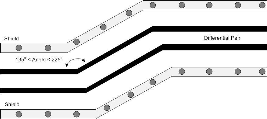
- Ensure that the bend angles associated with the differential signal pairs are between 135o and 225o (See Figure 10-13).
 Figure 10-13 FPD-Link Routing Example