SNLS604E September 2020 – November 2022 DP83TG720S-Q1
PRODUCTION DATA
- 1 Features
- 2 Applications
- 3 Description
- 4 Revision History
- 5 Pin Configuration and Functions
- 6 Specifications
-
7 Detailed Description
- 7.1 Overview
- 7.2 Functional Block Diagram
- 7.3 Feature Description
- 7.4
Device Functional Modes
- 7.4.1 Power Down
- 7.4.2 Reset
- 7.4.3 Standby
- 7.4.4 Normal
- 7.4.5 Sleep
- 7.4.6 State Transitions
- 7.4.7 Media Dependent Interface
- 7.4.8 MAC Interfaces
- 7.4.9 Serial Management Interface
- 7.4.10 Direct Register Access
- 7.4.11 Extended Register Space Access
- 7.4.12 Write Address Operation
- 7.4.13 Read Address Operation
- 7.4.14 Write Operation (No Post Increment)
- 7.4.15 Read Operation (No Post Increment)
- 7.4.16 Write Operation (Post Increment)
- 7.4.17 Read Operation (Post Increment)
- 7.5 Programming
- 7.6 Register Maps
- 8 Application and Implementation
- 9 Power Supply Recommendations
- 10Compatibility with TI's 100BT1 PHY
- 11Layout
- 12Device and Documentation Support
- 13Mechanical, Packaging, and Orderable Information
Package Options
Mechanical Data (Package|Pins)
- RHA|36
Thermal pad, mechanical data (Package|Pins)
- RHA|36
Orderable Information
7.4.8.2 Serial Gigabit Media Independent Interface
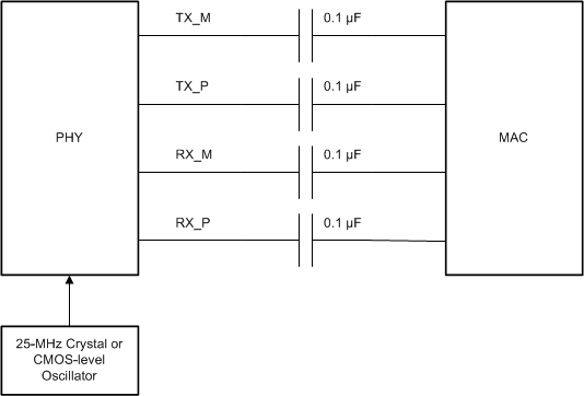
The Serial Gigabit Media Independent Interface (SGMII) provides a means for data transfer between MAC and PHY with significantly less signal pins (4 pins) compared to RGMII (12 pins). SGMII uses low-voltage differential signaling (LVDS) to reduce emissions and improve signal quality.
The DP83TG720S-Q1 SGMII is capable of operating in 4-wire mode. In 4-wire operation, two differential pairs are used to transmit and receive data. Clock and data recovery are performed in the MAC and in the PHY in the case of the RX and TX directions, respectively.
SGMII Auto-Negotitation can be disabled by setting bit[0] = 0b0 in the SGMII Configuration Register (SGMIICTL, address 0x608).
The SGMII signals are summarized in Table 7-13.
| FUNCTION | PINS |
|---|---|
| Data Signals | TX_M, TX_P |
| RX_M, RX_P |
 Figure 7-16 SGMII Connections
SGMII MAC Interface for Gigabit Ethernet has stringent signal integrity requirements to meet system level performance. It is advised to take the following requirements into consideration when designing PCB. It is also recommended to check board level signal integrity by using the DP83TG720 IBIS model.
SGMII Signals Guidelines
- Sgmii Tx and Rx signals should be routed on board with control differential impedance of 100ohms +/- 5%.
- Maximum routing length should be limited to 5inch for better signal integrity.
- Mismatch in routing length of p and n should be limited to 5mils.
- AC-coupling caps on rx lines should be placed close to rx_p and rx_m pins of PHY.
- AC-coupling caps on tx lines should be placed close to tx_p and tx_m pins of MAC.
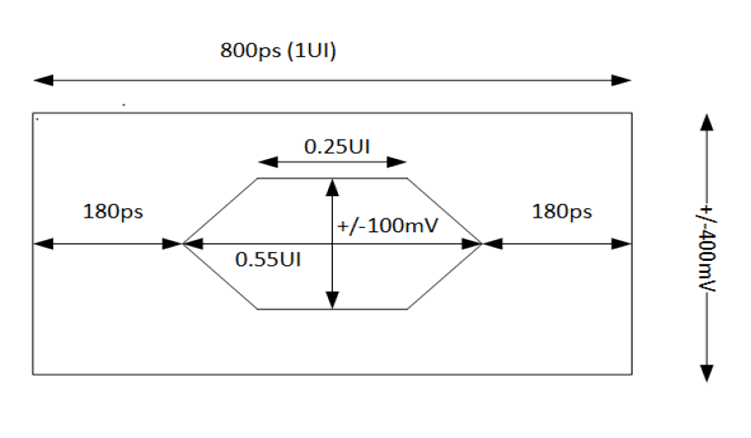
- Signal integrity should be checked only at the pins of the receiver (PHY or MAC) using the high speed differential probe.
- At PHY's TX_M and TX_P following eye mask should be
ensured :
 Figure 7-17 Sgmii PHY Receiver Mask
Requirement