SPRS950F December 2015 – May 2019 DRA744 , DRA745 , DRA746 , DRA750 , DRA756
PRODUCTION DATA.
- 1 Device Overview
- 2 Revision History
- 3 Device Comparison
-
4 Terminal Configuration and Functions
- 4.1 Terminal Assignment
- 4.2 Ball Characteristics
- 4.3 Multiplexing Characteristics
- 4.4
Signal Descriptions
- 4.4.1 Video Input Ports (VIP)
- 4.4.2 Display Subsystem – Video Output Ports
- 4.4.3 Display Subsystem – High-Definition Multimedia Interface (HDMI)
- 4.4.4 External Memory Interface (EMIF)
- 4.4.5 General-Purpose Memory Controller (GPMC)
- 4.4.6 Timers
- 4.4.7 Inter-Integrated Circuit Interface (I2C)
- 4.4.8 HDQ / 1-Wire Interface (HDQ1W)
- 4.4.9 Universal Asynchronous Receiver Transmitter (UART)
- 4.4.10 Multichannel Serial Peripheral Interface (McSPI)
- 4.4.11 Quad Serial Peripheral Interface (QSPI)
- 4.4.12 Multichannel Audio Serial Port (McASP)
- 4.4.13 Universal Serial Bus (USB)
- 4.4.14 SATA
- 4.4.15 Peripheral Component Interconnect Express (PCIe)
- 4.4.16 Controller Area Network Interface (DCAN)
- 4.4.17 Ethernet Interface (GMAC_SW)
- 4.4.18 Media Local Bus (MLB) Interface
- 4.4.19 eMMC/SD/SDIO
- 4.4.20 General-Purpose Interface (GPIO)
- 4.4.21 Keyboard controller (KBD)
- 4.4.22 Pulse Width Modulation (PWM) Interface
- 4.4.23 Audio Tracking Logic (ATL)
- 4.4.24 Test Interfaces
- 4.4.25 System and Miscellaneous
- 4.4.26 Power Supplies
-
5 Specifications
- 5.1 Absolute Maximum Ratings
- 5.2 ESD Ratings
- 5.3 Power on Hour (POH) Limits
- 5.4 Recommended Operating Conditions
- 5.5 Operating Performance Points
- 5.6 Power Consumption Summary
- 5.7
Electrical Characteristics
- 5.7.1 LVCMOS DDR DC Electrical Characteristics
- 5.7.2 HDMIPHY DC Electrical Characteristics
- 5.7.3 Dual Voltage LVCMOS I2C DC Electrical Characteristics
- 5.7.4 IQ1833 Buffers DC Electrical Characteristics
- 5.7.5 IHHV1833 Buffers DC Electrical Characteristics
- 5.7.6 LVCMOS OSC Buffers DC Electrical Characteristics
- 5.7.7 ILVDS18 Buffers DC Electrical Characteristics
- 5.7.8 BMLB18 Buffers DC Electrical Characteristics
- 5.7.9 BC1833IHHV Buffers DC Electrical Characteristics
- 5.7.10 USBPHY DC Electrical Characteristics
- 5.7.11 Dual Voltage SDIO1833 DC Electrical Characteristics
- 5.7.12 Dual Voltage LVCMOS DC Electrical Characteristics
- 5.7.13 SATAPHY DC Electrical Characteristics
- 5.7.14 PCIEPHY DC Electrical Characteristics
- 5.8 Thermal Resistance Characteristics
- 5.9 Power Supply Sequences
- 6 Clock Specifications
-
7 Timing Requirements and Switching Characteristics
- 7.1 Timing Test Conditions
- 7.2 Interface Clock Specifications
- 7.3 Timing Parameters and Information
- 7.4 Recommended Clock and Control Signal Transition Behavior
- 7.5 Virtual and Manual I/O Timing Modes
- 7.6 Video Input Ports (VIP)
- 7.7 Display Subsystem – Video Output Ports
- 7.8 Display Subsystem – High-Definition Multimedia Interface (HDMI)
- 7.9 External Memory Interface (EMIF)
- 7.10 General-Purpose Memory Controller (GPMC)
- 7.11 Timers
- 7.12 Inter-Integrated Circuit Interface (I2C)
- 7.13 HDQ / 1-Wire Interface (HDQ1W)
- 7.14 Universal Asynchronous Receiver Transmitter (UART)
- 7.15 Multichannel Serial Peripheral Interface (McSPI)
- 7.16 Quad Serial Peripheral Interface (QSPI)
- 7.17
Multichannel Audio Serial Port (McASP)
- Table 7-49 Timing Requirements for McASP1
- Table 7-50 Timing Requirements for McASP2
- Table 7-51 Timing Requirements for McASP3/4/5/6/7/8
- Table 7-52 Switching Characteristics Over Recommended Operating Conditions for McASP1
- Table 7-53 Switching Characteristics Over Recommended Operating Conditions for McASP2
- Table 7-54 Switching Characteristics Over Recommended Operating Conditions for McASP3/4/5/6/7/8
- 7.18 Universal Serial Bus (USB)
- 7.19 Serial Advanced Technology Attachment (SATA)
- 7.20 Peripheral Component Interconnect Express (PCIe)
- 7.21 Controller Area Network Interface (DCAN)
- 7.22
Ethernet Interface (GMAC_SW)
- 7.22.1
GMAC MII Timings
- Table 7-71 Timing Requirements for miin_rxclk - MII Operation
- Table 7-72 Timing Requirements for miin_txclk - MII Operation
- Table 7-73 Timing Requirements for GMAC MIIn Receive 10/100 Mbit/s
- Table 7-74 Switching Characteristics Over Recommended Operating Conditions for GMAC MIIn Transmit 10/100 Mbits/s
- 7.22.2 GMAC MDIO Interface Timings
- 7.22.3
GMAC RMII Timings
- Table 7-79 Timing Requirements for GMAC REF_CLK - RMII Operation
- Table 7-80 Timing Requirements for GMAC RMIIn Receive
- Table 7-81 Switching Characteristics Over Recommended Operating Conditions for GMAC REF_CLK - RMII Operation
- Table 7-82 Switching Characteristics Over Recommended Operating Conditions for GMAC RMIIn Transmit 10/100 Mbits/s
- 7.22.4
GMAC RGMII Timings
- Table 7-86 Timing Requirements for rgmiin_rxc - RGMIIn Operation
- Table 7-87 Timing Requirements for GMAC RGMIIn Input Receive for 10/100/1000 Mbps
- Table 7-88 Switching Characteristics Over Recommended Operating Conditions for rgmiin_txctl - RGMIIn Operation for 10/100/1000 Mbit/s
- Table 7-89 Switching Characteristics for GMAC RGMIIn Output Transmit for 10/100/1000 Mbps
- 7.22.1
GMAC MII Timings
- 7.23 Media Local Bus (MLB) interface
- 7.24
eMMC/SD/SDIO
- 7.24.1
MMC1—SD Card Interface
- 7.24.1.1 Default speed, 4-bit data, SDR, half-cycle
- 7.24.1.2 High speed, 4-bit data, SDR, half-cycle
- 7.24.1.3 SDR12, 4-bit data, half-cycle
- 7.24.1.4 SDR25, 4-bit data, half-cycle
- 7.24.1.5 UHS-I SDR50, 4-bit data, half-cycle
- 7.24.1.6 UHS-I SDR104, 4-bit data, half-cycle
- 7.24.1.7 UHS-I DDR50, 4-bit data
- 7.24.2 MMC2 — eMMC
- 7.24.3 MMC3 and MMC4—SDIO/SD
- 7.24.1
MMC1—SD Card Interface
- 7.25 General-Purpose Interface (GPIO)
- 7.26 Audio Tracking Logic (ATL)
- 7.27 System and Miscellaneous interfaces
- 7.28
Test Interfaces
- 7.28.1
IEEE 1149.1 Standard-Test-Access Port (JTAG)
- 7.28.1.1
JTAG Electrical Data/Timing
- Table 7-146 Timing Requirements for IEEE 1149.1 JTAG
- Table 7-147 Switching Characteristics Over Recommended Operating Conditions for IEEE 1149.1 JTAG
- Table 7-148 Timing Requirements for IEEE 1149.1 JTAG With RTCK
- Table 7-149 Switching Characteristics Over Recommended Operating Conditions for IEEE 1149.1 JTAG With RTCK
- 7.28.1.1
JTAG Electrical Data/Timing
- 7.28.2 Trace Port Interface Unit (TPIU)
- 7.28.1
IEEE 1149.1 Standard-Test-Access Port (JTAG)
-
8 Applications, Implementation, and Layout
- 8.1 Introduction
- 8.2 Power Optimizations
- 8.3 Core Power Domains
- 8.4 Single-Ended Interfaces
- 8.5
Differential Interfaces
- 8.5.1 General Routing Guidelines
- 8.5.2
USB 2.0 Board Design and Layout Guidelines
- 8.5.2.1 Background
- 8.5.2.2
USB PHY Layout Guide
- 8.5.2.2.1 General Routing and Placement
- 8.5.2.2.2
Specific Guidelines for USB PHY Layout
- 8.5.2.2.2.1 Analog, PLL, and Digital Power Supply Filtering
- 8.5.2.2.2.2 Analog, Digital, and PLL Partitioning
- 8.5.2.2.2.3 Board Stackup
- 8.5.2.2.2.4 Cable Connector Socket
- 8.5.2.2.2.5 Clock Routings
- 8.5.2.2.2.6 Crystals/Oscillator
- 8.5.2.2.2.7 DP/DM Trace
- 8.5.2.2.2.8 DP/DM Vias
- 8.5.2.2.2.9 Image Planes
- 8.5.2.2.2.10 JTAG Interface
- 8.5.2.2.2.11 Power Regulators
- 8.5.2.3 Electrostatic Discharge (ESD)
- 8.5.2.4 References
- 8.5.3 USB 3.0 Board Design and Layout Guidelines
- 8.5.4 HDMI Board Design and Layout Guidelines
- 8.5.5 SATA Board Design and Layout Guidelines
- 8.5.6 PCIe Board Design and Layout Guidelines
- 8.6 Clock Routing Guidelines
- 8.7
DDR2/DDR3 Board Design and Layout Guidelines
- 8.7.1 DDR2/DDR3 General Board Layout Guidelines
- 8.7.2 DDR2 Board Design and Layout Guidelines
- 8.7.3
DDR3 Board Design and Layout Guidelines
- 8.7.3.1 Board Designs
- 8.7.3.2 DDR3 EMIFs
- 8.7.3.3 DDR3 Device Combinations
- 8.7.3.4 DDR3 Interface Schematic
- 8.7.3.5 Compatible JEDEC DDR3 Devices
- 8.7.3.6 PCB Stackup
- 8.7.3.7 Placement
- 8.7.3.8 DDR3 Keepout Region
- 8.7.3.9 Bulk Bypass Capacitors
- 8.7.3.10 High-Speed Bypass Capacitors
- 8.7.3.11 Net Classes
- 8.7.3.12 DDR3 Signal Termination
- 8.7.3.13 VREF_DDR Routing
- 8.7.3.14 VTT
- 8.7.3.15 CK and ADDR_CTRL Topologies and Routing Definition
- 8.7.3.16 Data Topologies and Routing Definition
- 8.7.3.17 Routing Specification
- 9 Device and Documentation Support
- 10Mechanical, Packaging, and Orderable Information
Package Options
Refer to the PDF data sheet for device specific package drawings
Mechanical Data (Package|Pins)
- ABC|760
Thermal pad, mechanical data (Package|Pins)
Orderable Information
8.2.2 Step 2: Physical Placement
A critical step in designing an optimized PDN is that proper care must be taken to making sure that the initial floor planning of the PCB layout is done with good power integrity design guidelines in mind. The following points are important for optimizing a PCB’s PDN:
- Minimizing the physical distance between power sources and key high load components is the first step toward optimization. Placing source and load components on the same side of the PCB is desirable. This will minimize via inductance impact for high current loads and steps
- External trace routing between components must be as wide as possible. The wider the traces, the lower the DC resistance and consequently the lower the static IR drop.
- Whenever possible for the internal layers (routing and plane), wide traces and copper area fills are preferred for PDN layout. The routing of power nets in plane provide for more interplane capacitance and improved high frequency performance of the PDN.
- Whenever possible, use a via to component pin/pad ratio of 1:1 or better (i.e. especially decoupling capacitors, power inductors and current sensing resistors). Do not share vias among multiple capacitors for connecting power supply and ground planes.
- Placement of vias must be as close as possible or even within a component’s solder pad if the PCB technology you are using provides this capability.
- To avoid any “ampacity” issue – maximum current-carrying capacity of each transitional via should be evaluated to determine the appropriate number of vias required to connect components.
Figure 8-4 shows an example of acceptable width for power net routing but with poor via placement.
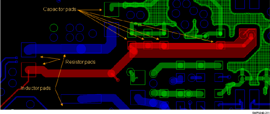 Figure 8-4 Poor Via Assignment for PDN
 Figure 8-5 shows an improved power net routing with better via assignment and placement, respectively.
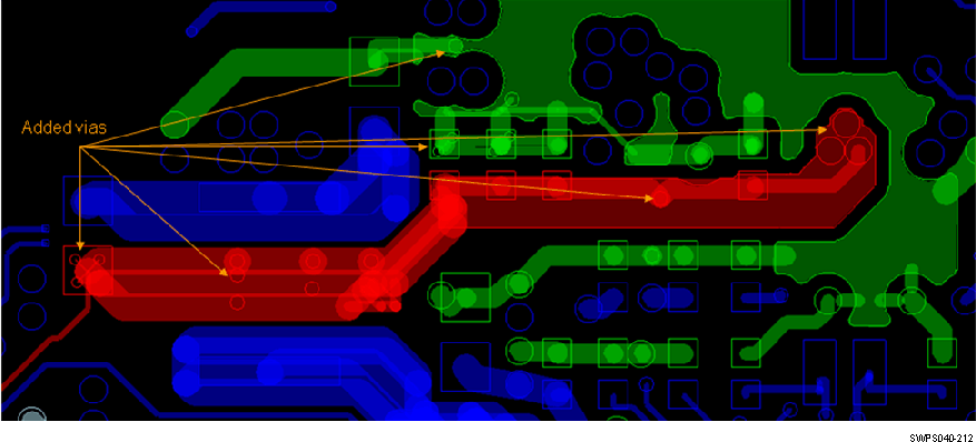 Figure 8-5 Improved Via Assignment for PDN
 Figure 8-6 and Figure 8-7 show examples of “via starvation” on a power net transitioning from top routing layer to internal layers and the improved layout, respectively. Adding vias to bring the “via-to-pad” ratio to 1:1 will improve PDN performance.
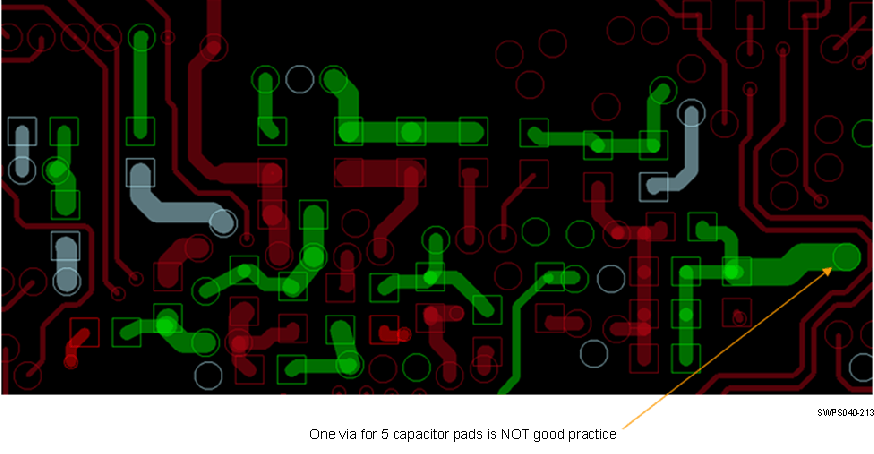 Figure 8-6 Via Starvation
 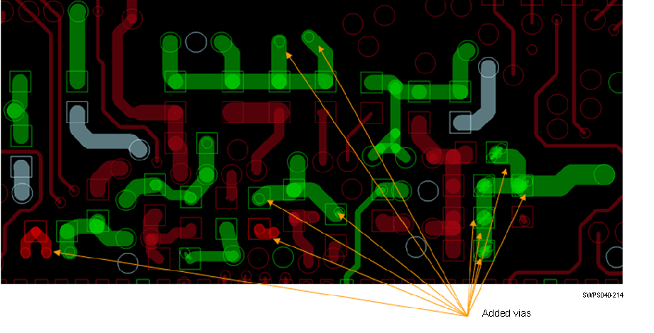 Figure 8-7 Improved Layout With More Transitional Vias
 - For noise sensitive power supplies (i.e. Phase Lock-Loops, analog signals like audio and video), a Gnd shield can be used to isolate coplanar supplies that may have high step currents or high frequency switching transitions from coupling into low-noise supplies.
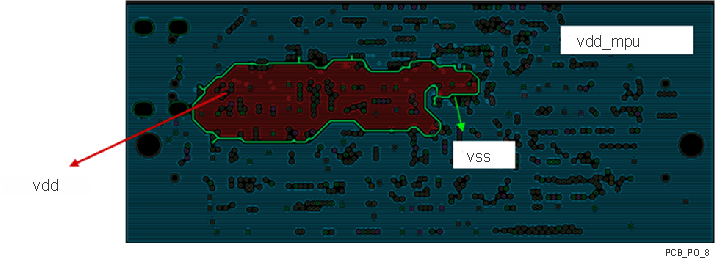 Figure 8-8 Coplanar Shielding of Power Net Using Ground Guard-band