SLVSD14A June   2017  – June  2020 DRV10983-Q1

PRODUCTION DATA.  

  1. Features
  2. Applications
  3. Description
    1.     Application Schematic
  4. Revision History
  5. Description (Continued)
  6. Pin Configuration and Functions
    1.     Pin Functions
  7. Specifications
    1. 7.1 Absolute Maximum Ratings
    2. 7.2 ESD Ratings
    3. 7.3 Recommended Operating Conditions
    4. 7.4 Thermal Information
    5. 7.5 Electrical Characteristics
    6. 7.6 Typical Characteristics
  8. Detailed Description
    1. 8.1 Overview
    2. 8.2 Functional Block Diagram
    3. 8.3 Feature Description
      1. 8.3.1 Regulators
        1. 8.3.1.1 Step-Down Regulator
        2. 8.3.1.2 3.3-V and 1.8-V LDO
      2. 8.3.2 Protection Circuits
        1. 8.3.2.1 Thermal Shutdown
        2. 8.3.2.2 Undervoltage Lockout (UVLO)
        3. 8.3.2.3 Overcurrent Protection
        4. 8.3.2.4 Lock
      3. 8.3.3 Motor Speed Control
      4. 8.3.4 Load Dump Handling
      5. 8.3.5 Sleep or Standby Condition
        1. 8.3.5.1 Required Sequence to Enter Sleep Mode
          1. 8.3.5.1.1 Option 1
          2. 8.3.5.1.2 Option 2
      6. 8.3.6 EEPROM Access
    4. 8.4 Device Functional Modes
      1. 8.4.1  Motor Parameters
        1. 8.4.1.1 Motor Phase Resistance
        2. 8.4.1.2 BEMF Constant
      2. 8.4.2  Starting the Motor Under Different Initial Conditions
        1. 8.4.2.1 Case 1 – Motor is Stationary
        2. 8.4.2.2 Case 2 – Motor is Spinning in the Forward Direction
        3. 8.4.2.3 Case 3 – Motor is Spinning in the Reverse Direction
      3. 8.4.3  Motor Start Sequence
        1. 8.4.3.1 Initial Speed Detect
        2. 8.4.3.2 Motor Resynchronization
        3. 8.4.3.3 Reverse Drive
        4. 8.4.3.4 Motor Brake
        5. 8.4.3.5 Motor Initialization
          1. 8.4.3.5.1 Align
          2. 8.4.3.5.2 Initial Position Detect (IPD)
            1. 8.4.3.5.2.1 IPD Operation
            2. 8.4.3.5.2.2 IPD Release Mode
            3. 8.4.3.5.2.3 IPD Advance Angle
          3. 8.4.3.5.3 Motor Start
        6. 8.4.3.6 Start-Up Timing
      4. 8.4.4  Align Current
      5. 8.4.5  Start-Up Current Setting
        1. 8.4.5.1 Start-Up Current Ramp-Up
      6. 8.4.6  Closed Loop
        1. 8.4.6.1 Half-Cycle Control and Full-Cycle Control
        2. 8.4.6.2 Analog-Mode Speed Control
        3. 8.4.6.3 Digital PWM-Input-Mode Speed Control
        4. 8.4.6.4 I2C-Mode Speed Control
        5. 8.4.6.5 Closed-Loop Accelerate
        6. 8.4.6.6 Control Coefficient
        7. 8.4.6.7 Commutation Control Advance Angle
      7. 8.4.7  Current Limit
        1. 8.4.7.1 Acceleration Current Limit
      8. 8.4.8  Lock Detect and Fault Handling
        1. 8.4.8.1 Lock0: Lock-Detection Current Limit Triggered
        2. 8.4.8.2 Lock1: Abnormal Speed
        3. 8.4.8.3 Lock2: Abnormal Kt
        4. 8.4.8.4 Lock3 (Fault3): No-Motor Fault
        5. 8.4.8.5 Lock4: Open-Loop Motor-Stuck Lock
        6. 8.4.8.6 Lock5: Closed Loop Motor Stuck Lock
      9. 8.4.9  Anti Voltage Suppression Function
        1. 8.4.9.1 Mechanical AVS Function
        2. 8.4.9.2 Inductive AVS Function
      10. 8.4.10 PWM Output
      11. 8.4.11 FG Customized Configuration
        1. 8.4.11.1 FG Output Frequency
        2. 8.4.11.2 FG Open Loop and Lock Behavior
      12. 8.4.12 Diagnostics and Visibility
        1. 8.4.12.1 Motor-Status Readback
        2. 8.4.12.2 Motor-Speed Readback
        3. 8.4.12.3 Motor Electrical-Period Readback
        4. 8.4.12.4 BEMF Constant Read Back
        5. 8.4.12.5 Motor Estimated Position by IPD
        6. 8.4.12.6 Supply-Voltage Readback
        7. 8.4.12.7 Speed-Command Readback
        8. 8.4.12.8 Speed-Command Buffer Readback
        9. 8.4.12.9 Fault Diagnostics
    5. 8.5 Register Maps
      1. 8.5.1 I2C Serial Interface
      2. 8.5.2 Register Map
      3. 8.5.3 Register Descriptions
        1. 8.5.3.1  FaultReg Register (address = 0x00) [reset = 0x00]
          1. Table 11. FaultReg Register Field Descriptions
        2. 8.5.3.2  MotorSpeed Register (address = 0x01) [reset = 0x00]
          1. Table 12. MotorSpeed Register Field Descriptions
        3. 8.5.3.3  MotorPeriod Register (address = 0x02) [reset = 0x00]
          1. Table 13. MotorPeriod Register Field Descriptions
        4. 8.5.3.4  MotorKt Register (address = 0x03) [reset = 0x00]
          1. Table 14. MotorKt Register Field Descriptions
        5. 8.5.3.5  MotorCurrent Register (address = 0x04) [reset = 0x00]
          1. Table 15. MotorCurrent Register Field Descriptions
        6. 8.5.3.6  IPDPosition–SupplyVoltage Register (address = 0x05) [reset = 0x00]
          1. Table 16. IPDPosition–SupplyVoltage Register Field Descriptions
        7. 8.5.3.7  SpeedCmd–spdCmdBuffer Register (address = 0x06) [reset = 0x00]
          1. Table 17. SpeedCmd–spdCmdBuffer Register Field Descriptions
        8. 8.5.3.8  AnalogInLvl Register (address = 0x07) [reset = 0x00]
          1. Table 18. AnalogInLvl Register Field Descriptions
        9. 8.5.3.9  DeviceID–RevisionID Register (address = 0x08) [reset = 0x00]
          1. Table 19. DeviceID–RevisionID Register Field Descriptions
        10. 8.5.3.10 DeviceID–RevisionID Register (address = 0x08) [reset = 0x00]
          1. Table 20. DeviceID–RevisionID Register Field Descriptions
        11. 8.5.3.11 Unused Registers (addresses = 0x011 Through 0x2F)
        12. 8.5.3.12 SpeedCtrl Register (address = 0x30) [reset = 0x00]
          1. Table 21. SpeedCtrl Register Field Descriptions
        13. 8.5.3.13 EEPROM Programming1 Register (address = 0x31) [reset = 0x00]
          1. Table 22. EEPROM Programming1 Register Field Descriptions
        14. 8.5.3.14 EEPROM Programming2 Register (address = 0x32) [reset = 0x00]
          1. Table 23. EEPROM Programming2 Register Field Descriptions
        15. 8.5.3.15 EEPROM Programming3 Register (address = 0x33) [reset = 0x00]
          1. Table 24. EEPROM Programming3 Register Field Descriptions
        16. 8.5.3.16 EEPROM Programming4 Register (address = 0x34) [reset = 0x00]
          1. Table 25. EEPROM Programming4 Register Field Descriptions
        17. 8.5.3.17 EEPROM Programming5 Register (address = 0x35) [reset = 0x00]
          1. Table 26. EEPROM Programming5 Register Field Descriptions
        18. 8.5.3.18 EEPROM Programming6 Register (address = 0x36) [reset = 0x00]
          1. Table 27. EEPROM Programming6 Register Field Descriptions
        19. 8.5.3.19 Unused Registers (addresses = 0x37 Through 0x5F)
        20. 8.5.3.20 EECTRL Register (address = 0x60) [reset = 0x00]
          1. Table 28. EECTRL Register Field Descriptions
        21. 8.5.3.21 Unused Registers (addresses = 0x61 Through 0x8F)
        22. 8.5.3.22 CONFIG1 Register (address = 0x90) [reset = 0x00]
          1. Table 29. CONFIG1 Register Field Descriptions
        23. 8.5.3.23 CONFIG2 Register (address = 0x91) [reset = 0x00]
          1. Table 30. CONFIG2 Register Field Descriptions
        24. 8.5.3.24 CONFIG3 Register (address = 0x92) [reset = 0x00]
          1. Table 31. CONFIG3 Register Field Descriptions
        25. 8.5.3.25 CONFIG4 Register (address = 0x93) [reset = 0x00]
          1. Table 32. CONFIG4 Register Field Descriptions
        26. 8.5.3.26 CONFIG5 Register (address = 0x94) [reset = 0x00]
          1. Table 33. CONFIG5 Register Field Descriptions
        27. 8.5.3.27 CONFIG6 Register (address = 0x95) [reset = 0x00]
          1. Table 34. CONFIG6 Register Field Descriptions
        28. 8.5.3.28 CONFIG7 Register (address = 0x96) [reset = 0x00]
          1. Table 35. CONFIG7 Register Field Descriptions
  9. Application and Implementation
    1. 9.1 Application Information
    2. 9.2 Typical Application
      1. 9.2.1 Design Requirements
      2. 9.2.2 Detailed Design Procedure
      3. 9.2.3 Application Curves
  10. 10Power Supply Recommendations
  11. 11Layout
    1. 11.1 Layout Guidelines
    2. 11.2 Layout Example
  12. 12Device and Documentation Support
    1. 12.1 Trademarks
    2. 12.2 Electrostatic Discharge Caution
    3. 12.3 Receiving Notification of Documentation Updates
    4. 12.4 Community Resources
    5. 12.5 Glossary
  13. 13Mechanical, Packaging, and Orderable Information

Package Options

Mechanical Data (Package|Pins)
Thermal pad, mechanical data (Package|Pins)
Orderable Information

BEMF Constant

The BEMF constant, Kt[6:0] describes the phase-to-phase BEMF voltage of the motor as a function of the motor velocity.

Figure 15 shows the measurement technique for this constant as used in the DRV10983-Q1 device.
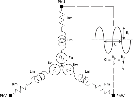
DRV10983-Q1 Kt_PH_def_SLVSD14.gifFigure 15. KtPH Definition

With the motor coasting, use an oscilloscope to capture the differential voltage waveform between any two phases. Derive the BEMF constant used by the DRV10983-Q1 device as shown in Equation 1.

Equation 1. KtPH = Ep × te

where

  • Ep is ½ the peak-to-peak amplitude of the measured voltage
  • te is the electrical period

The measured BEMF constant (KtPH) must be converted to a 7-bit digital register value Kt[6:0] (combination of KtShift[2:0] and KtValue[3:0]) to program the BEMF constant value. The digital register value can be determined as follows:

  1. Convert the measured KtPH to a weighted digital value: Ktph_dig = 1090 × KtPH
  2. Encode the digital value such that Ktph_dig = KtValue[3:0] << KtShift[2:0].

The maximum KtPH that can be programmed is 1760 mV/Hz. This represents a digital value of 1920 and an encoded Kt[6:0] value of 0x7Fh. The minimum KtPH that can be programmed is 0.92 mV/Hz, which represents a digital value of 1 and an encoded Kt[6:0] value of 0x01h.

For convenience, the encoded value of Kt[6:0] may also be obtained from Table 4.

Table 4. BEMF Constant Look-Up Table

Kt[6:0] {KtShift[2:0], KtValue[3:0]} KtPH (mV/Hz) Kt [6:0] {KtShift[2:0], KtValue[3:0]} KtPH (mV/Hz) Kt [6:0] {KtShift[2:0], KtValue[3:0]} KtPH (mV/Hz)
BINARY HEX BINARY HEX BINARY HEX
000 0000 0x00 0 010 1000 0x28 29.44 101 1000 0x58 235.52
000 0001 0x01 0.92 010 1001 0x29 33.12 101 1001 0x59 264.96
000 0010 0x02 1.84 010 1010 0x2A 36.8 101 1010 0x5A 294.4
000 0011 0x03 2.76 010 1011 0x2B 40.48 101 1011 0x5B 323.84
000 0100 0x04 3.68 010 1100 0x2C 44.16 101 1100 0x5C 353.28
000 0101 0x05 4.6 010 1101 0x2D 47.84 101 1101 0x5D 382.72
000 0110 0x06 5.52 010 1110 0x2E 51.52 101 1110 0x5E 412.16
000 0111 0x07 6.44 010 1111 0x2F 55.2 101 1111 0x5F 441.6
000 1000 0x08 7.36 011 1000 0x38 58.88 110 1000 0x68 471.04
000 1001 0x09 8.28 011 1001 0x39 66.24 110 1001 0x69 529.92
000 1010 0x0A 9.2 011 1010 0x3A 73.6 110 1010 0x6A 588.8
000 1011 0x0B 10.12 011 1011 0x3B 80.96 110 1011 0x6B 647.68
000 1100 0x0C 11.04 011 1100 0x3C 88.32 110 1100 0x6C 706.56
000 1101 0x0D 11.96 011 1101 0x3D 95.68 110 1101 0x6D 765.44
000 1110 0x0E 12.88 011 1110 0x3E 103.04 110 1110 0x6E 824.32
000 1111 0x0F 13.8 011 1111 0x3F 110.4 110 1111 0x6F 883.2
001 1000 0x18 14.72 100 1000 0x48 117.76 111 1000 0x78 942.08
001 1001 0x19 16.56 100 1001 0x49 132.48 111 1001 0x79 1059.84
001 1010 0x1A 18.4 100 1010 0x4A 147.2 111 1010 0x7A 1177.6
001 1011 0x1B 20.24 100 1011 0x4B 161.92 111 1011 0x7B 1295.36
001 1100 0x1C 22.08 100 1100 0x4C 176.64 111 1100 0x7C 1413.12
001 1101 0x1D 23.92 100 1101 0x4D 191.36 111 1101 0x7D 1530.88
001 1110 0x1E 25.76 100 1110 0x4E 206.08 111 1110 0x7E 1648.64
001 1111 0x1F 27.6 100 1111 0x4F 220.8 111 1111 0x7F 1766.4