SLVSD14A June   2017  – June  2020 DRV10983-Q1

PRODUCTION DATA.  

  1. Features
  2. Applications
  3. Description
    1.     Application Schematic
  4. Revision History
  5. Description (Continued)
  6. Pin Configuration and Functions
    1.     Pin Functions
  7. Specifications
    1. 7.1 Absolute Maximum Ratings
    2. 7.2 ESD Ratings
    3. 7.3 Recommended Operating Conditions
    4. 7.4 Thermal Information
    5. 7.5 Electrical Characteristics
    6. 7.6 Typical Characteristics
  8. Detailed Description
    1. 8.1 Overview
    2. 8.2 Functional Block Diagram
    3. 8.3 Feature Description
      1. 8.3.1 Regulators
        1. 8.3.1.1 Step-Down Regulator
        2. 8.3.1.2 3.3-V and 1.8-V LDO
      2. 8.3.2 Protection Circuits
        1. 8.3.2.1 Thermal Shutdown
        2. 8.3.2.2 Undervoltage Lockout (UVLO)
        3. 8.3.2.3 Overcurrent Protection
        4. 8.3.2.4 Lock
      3. 8.3.3 Motor Speed Control
      4. 8.3.4 Load Dump Handling
      5. 8.3.5 Sleep or Standby Condition
        1. 8.3.5.1 Required Sequence to Enter Sleep Mode
          1. 8.3.5.1.1 Option 1
          2. 8.3.5.1.2 Option 2
      6. 8.3.6 EEPROM Access
    4. 8.4 Device Functional Modes
      1. 8.4.1  Motor Parameters
        1. 8.4.1.1 Motor Phase Resistance
        2. 8.4.1.2 BEMF Constant
      2. 8.4.2  Starting the Motor Under Different Initial Conditions
        1. 8.4.2.1 Case 1 – Motor is Stationary
        2. 8.4.2.2 Case 2 – Motor is Spinning in the Forward Direction
        3. 8.4.2.3 Case 3 – Motor is Spinning in the Reverse Direction
      3. 8.4.3  Motor Start Sequence
        1. 8.4.3.1 Initial Speed Detect
        2. 8.4.3.2 Motor Resynchronization
        3. 8.4.3.3 Reverse Drive
        4. 8.4.3.4 Motor Brake
        5. 8.4.3.5 Motor Initialization
          1. 8.4.3.5.1 Align
          2. 8.4.3.5.2 Initial Position Detect (IPD)
            1. 8.4.3.5.2.1 IPD Operation
            2. 8.4.3.5.2.2 IPD Release Mode
            3. 8.4.3.5.2.3 IPD Advance Angle
          3. 8.4.3.5.3 Motor Start
        6. 8.4.3.6 Start-Up Timing
      4. 8.4.4  Align Current
      5. 8.4.5  Start-Up Current Setting
        1. 8.4.5.1 Start-Up Current Ramp-Up
      6. 8.4.6  Closed Loop
        1. 8.4.6.1 Half-Cycle Control and Full-Cycle Control
        2. 8.4.6.2 Analog-Mode Speed Control
        3. 8.4.6.3 Digital PWM-Input-Mode Speed Control
        4. 8.4.6.4 I2C-Mode Speed Control
        5. 8.4.6.5 Closed-Loop Accelerate
        6. 8.4.6.6 Control Coefficient
        7. 8.4.6.7 Commutation Control Advance Angle
      7. 8.4.7  Current Limit
        1. 8.4.7.1 Acceleration Current Limit
      8. 8.4.8  Lock Detect and Fault Handling
        1. 8.4.8.1 Lock0: Lock-Detection Current Limit Triggered
        2. 8.4.8.2 Lock1: Abnormal Speed
        3. 8.4.8.3 Lock2: Abnormal Kt
        4. 8.4.8.4 Lock3 (Fault3): No-Motor Fault
        5. 8.4.8.5 Lock4: Open-Loop Motor-Stuck Lock
        6. 8.4.8.6 Lock5: Closed Loop Motor Stuck Lock
      9. 8.4.9  Anti Voltage Suppression Function
        1. 8.4.9.1 Mechanical AVS Function
        2. 8.4.9.2 Inductive AVS Function
      10. 8.4.10 PWM Output
      11. 8.4.11 FG Customized Configuration
        1. 8.4.11.1 FG Output Frequency
        2. 8.4.11.2 FG Open Loop and Lock Behavior
      12. 8.4.12 Diagnostics and Visibility
        1. 8.4.12.1 Motor-Status Readback
        2. 8.4.12.2 Motor-Speed Readback
        3. 8.4.12.3 Motor Electrical-Period Readback
        4. 8.4.12.4 BEMF Constant Read Back
        5. 8.4.12.5 Motor Estimated Position by IPD
        6. 8.4.12.6 Supply-Voltage Readback
        7. 8.4.12.7 Speed-Command Readback
        8. 8.4.12.8 Speed-Command Buffer Readback
        9. 8.4.12.9 Fault Diagnostics
    5. 8.5 Register Maps
      1. 8.5.1 I2C Serial Interface
      2. 8.5.2 Register Map
      3. 8.5.3 Register Descriptions
        1. 8.5.3.1  FaultReg Register (address = 0x00) [reset = 0x00]
          1. Table 11. FaultReg Register Field Descriptions
        2. 8.5.3.2  MotorSpeed Register (address = 0x01) [reset = 0x00]
          1. Table 12. MotorSpeed Register Field Descriptions
        3. 8.5.3.3  MotorPeriod Register (address = 0x02) [reset = 0x00]
          1. Table 13. MotorPeriod Register Field Descriptions
        4. 8.5.3.4  MotorKt Register (address = 0x03) [reset = 0x00]
          1. Table 14. MotorKt Register Field Descriptions
        5. 8.5.3.5  MotorCurrent Register (address = 0x04) [reset = 0x00]
          1. Table 15. MotorCurrent Register Field Descriptions
        6. 8.5.3.6  IPDPosition–SupplyVoltage Register (address = 0x05) [reset = 0x00]
          1. Table 16. IPDPosition–SupplyVoltage Register Field Descriptions
        7. 8.5.3.7  SpeedCmd–spdCmdBuffer Register (address = 0x06) [reset = 0x00]
          1. Table 17. SpeedCmd–spdCmdBuffer Register Field Descriptions
        8. 8.5.3.8  AnalogInLvl Register (address = 0x07) [reset = 0x00]
          1. Table 18. AnalogInLvl Register Field Descriptions
        9. 8.5.3.9  DeviceID–RevisionID Register (address = 0x08) [reset = 0x00]
          1. Table 19. DeviceID–RevisionID Register Field Descriptions
        10. 8.5.3.10 DeviceID–RevisionID Register (address = 0x08) [reset = 0x00]
          1. Table 20. DeviceID–RevisionID Register Field Descriptions
        11. 8.5.3.11 Unused Registers (addresses = 0x011 Through 0x2F)
        12. 8.5.3.12 SpeedCtrl Register (address = 0x30) [reset = 0x00]
          1. Table 21. SpeedCtrl Register Field Descriptions
        13. 8.5.3.13 EEPROM Programming1 Register (address = 0x31) [reset = 0x00]
          1. Table 22. EEPROM Programming1 Register Field Descriptions
        14. 8.5.3.14 EEPROM Programming2 Register (address = 0x32) [reset = 0x00]
          1. Table 23. EEPROM Programming2 Register Field Descriptions
        15. 8.5.3.15 EEPROM Programming3 Register (address = 0x33) [reset = 0x00]
          1. Table 24. EEPROM Programming3 Register Field Descriptions
        16. 8.5.3.16 EEPROM Programming4 Register (address = 0x34) [reset = 0x00]
          1. Table 25. EEPROM Programming4 Register Field Descriptions
        17. 8.5.3.17 EEPROM Programming5 Register (address = 0x35) [reset = 0x00]
          1. Table 26. EEPROM Programming5 Register Field Descriptions
        18. 8.5.3.18 EEPROM Programming6 Register (address = 0x36) [reset = 0x00]
          1. Table 27. EEPROM Programming6 Register Field Descriptions
        19. 8.5.3.19 Unused Registers (addresses = 0x37 Through 0x5F)
        20. 8.5.3.20 EECTRL Register (address = 0x60) [reset = 0x00]
          1. Table 28. EECTRL Register Field Descriptions
        21. 8.5.3.21 Unused Registers (addresses = 0x61 Through 0x8F)
        22. 8.5.3.22 CONFIG1 Register (address = 0x90) [reset = 0x00]
          1. Table 29. CONFIG1 Register Field Descriptions
        23. 8.5.3.23 CONFIG2 Register (address = 0x91) [reset = 0x00]
          1. Table 30. CONFIG2 Register Field Descriptions
        24. 8.5.3.24 CONFIG3 Register (address = 0x92) [reset = 0x00]
          1. Table 31. CONFIG3 Register Field Descriptions
        25. 8.5.3.25 CONFIG4 Register (address = 0x93) [reset = 0x00]
          1. Table 32. CONFIG4 Register Field Descriptions
        26. 8.5.3.26 CONFIG5 Register (address = 0x94) [reset = 0x00]
          1. Table 33. CONFIG5 Register Field Descriptions
        27. 8.5.3.27 CONFIG6 Register (address = 0x95) [reset = 0x00]
          1. Table 34. CONFIG6 Register Field Descriptions
        28. 8.5.3.28 CONFIG7 Register (address = 0x96) [reset = 0x00]
          1. Table 35. CONFIG7 Register Field Descriptions
  9. Application and Implementation
    1. 9.1 Application Information
    2. 9.2 Typical Application
      1. 9.2.1 Design Requirements
      2. 9.2.2 Detailed Design Procedure
      3. 9.2.3 Application Curves
  10. 10Power Supply Recommendations
  11. 11Layout
    1. 11.1 Layout Guidelines
    2. 11.2 Layout Example
  12. 12Device and Documentation Support
    1. 12.1 Trademarks
    2. 12.2 Electrostatic Discharge Caution
    3. 12.3 Receiving Notification of Documentation Updates
    4. 12.4 Community Resources
    5. 12.5 Glossary
  13. 13Mechanical, Packaging, and Orderable Information

Package Options

Mechanical Data (Package|Pins)
Thermal pad, mechanical data (Package|Pins)
Orderable Information

Lock Detect and Fault Handling

The DRV10983-Q1 device provides several options for determining if the motor becomes locked as a result of some external torque. Five lock-detect schemes work together to ensure the lock condition is detected quickly and reliably. Figure 33 shows the logic which integrates the various lock-detect schemes. When a lock condition is detected, the DRV10983-Q1 device takes action to prevent continuously driving the motor in order to prevent damage to the system or the motor.

In addition to detecting if there is a locked motor condition, the DRV10983-Q1 device also identifies and takes action if there is no motor connected to the system.

Each of the five lock-detect schemes and the no-motor detection can be disabled by respective register bits LockEn[5:0].

When a lock condition is detected, the FaultReg register provides an indication of which of the six different conditions was detected on Lock5 to Lock0. These bits are reset when the motor restarts. The bits in the FaultReg register are set even if the lock detect scheme is disabled.

The DRV10983-Q1 device reacts to either locked-rotor or no-motor-connected conditions by putting the output drivers into a high-impedance state. To prevent the energy in the motor from pumping the supply voltage, the DRV10983-Q1 device incorporates an anti-voltage-surge (AVS) process whenever the output stages transition into the high-impedance state. The AVS function is described in Anti Voltage Suppression Function. After entering the high-impedance state as a result of a fault condition, the system tries to restart after tLOCK_OFF.
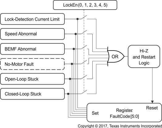
DRV10983-Q1 lock_det_fault_diag_SLVSD14.gifFigure 33. Lock Detect and Fault Diagnose