SLOS893D September 2014 – August 2025 DRV2624
PRODUCTION DATA
- 1
- 1 Features
- 2 Applications
- 3 Description
- 4 Pin Configuration and Functions
- 5 Specifications
- 6 Parameter Measurement Information
-
7 Detailed Description
- 7.1 Overview
- 7.2 Functional Block Diagram
- 7.3
Feature Description
- 7.3.1 Support for ERM and LRA Actuators
- 7.3.2 Smart-Loop Architecture
- 7.3.3 Open-Loop Operation
- 7.3.4 Flexible Front-End Interface
- 7.3.5 Noise Gate Control
- 7.3.6 Edge Rate Control
- 7.3.7 Constant Vibration Strength
- 7.3.8 Battery Voltage Reporting
- 7.3.9 Ultra Low-Power Shutdown
- 7.3.10 Automatic Go-To-Stand-by (Low Power)
- 7.3.11 I2C Watchdog Timer
- 7.3.12 Device Protection
- 7.3.13 POR
- 7.3.14 Silicon Revision Control
- 7.3.15 Support for LRA and ERM Actuators
- 7.3.16 Multi-Purpose Pin Functionality
- 7.3.17 Automatic Transition to Standby State
- 7.3.18 Automatic Brake into Standby
- 7.3.19 Battery Monitoring and Power Preservation
- 7.4 Device Functional Modes
- 7.5 Operation During Exceptional Conditions
- 7.6
Programming
- 7.6.1 Auto-Resonance Engine Programming for the LRA
- 7.6.2 Automatic-Level Calibration Programming
- 7.6.3 I2C Interface
- 7.6.4 Programming for Open-Loop Operation
- 7.6.5 Programming for Closed-Loop Operation
- 7.6.6 Diagnostics Routine
- 7.6.7 Calibration Routine
- 7.6.8 Waveform Playback Programming
- 7.6.9 Waveform Setup and Playback
- 7.6.10 120
-
8 Register Map
- 8.1 Address: 0x00
- 8.2 Address: 0x01
- 8.3 Address: 0x02
- 8.4 Address: 0x03
- 8.5 Address: 0x04
- 8.6 Address: 0x05
- 8.7 Address: 0x06
- 8.8 Address: 0x07
- 8.9 Address: 0x08
- 8.10 Address: 0x09
- 8.11 Address: 0x0A
- 8.12 Address: 0x0B
- 8.13 Address: 0x0C
- 8.14 Address: 0x0D
- 8.15 Address: 0x0E
- 8.16 Address: 0x0F
- 8.17 Address: 0x10
- 8.18 Address: 0x11
- 8.19 Address: 0x12
- 8.20 Address: 0x13
- 8.21 Address: 0x14
- 8.22 Address: 0x15
- 8.23 Address: 0x16
- 8.24 Address: 0x17
- 8.25 Address: 0x18
- 8.26 Address: 0x19
- 8.27 Address: 0x1A
- 8.28 Address: 0x1B
- 8.29 Address: 0x1C
- 8.30 Address: 0x1D
- 8.31 Address: 0x1F
- 8.32 Address: 0x20
- 8.33 Address: 0x21
- 8.34 Address: 0x22
- 8.35 Address: 0x23
- 8.36 Address: 0x24
- 8.37 Address: 0x25
- 8.38 Address: 0x26
- 8.39 Address: 0x27
- 8.40 Address: 0x28
- 8.41 Address: 0x29
- 8.42 Address: 0x2A
- 8.43 Address: 0x2C
- 8.44 Address: 0x2E
- 8.45 Address: 0x2F
- 8.46 Address: 0x30
- 8.47 Address: 0xFD
- 8.48 Address: 0xFE
- 8.49 Address: 0xFF
- Application and Implementation
- 9 Device and Documentation Support
- 10Revision History
- 11Mechanical, Packaging, and Orderable Information
Package Options
Refer to the PDF data sheet for device specific package drawings
Mechanical Data (Package|Pins)
- YFF|9
Thermal pad, mechanical data (Package|Pins)
Orderable Information
4 Pin Configuration and Functions
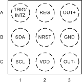
 Figure 4-1 YFF Package9-Pin DSBGATop View
Table 4-1 Pin Functions
| PIN | I/O | DESCRIPTION | |
|---|---|---|---|
| NAME | NO. | ||
| VDD | C2 | P | Supply input (2.7V to 5.5V). A 0.1µF capacitor is required. |
| GND | B3 | P | Supply ground |
| REG | A2 | O | 1.8V regulator output. A 0.1µF capacitor is required |
| OUT- | C3 | O | Negative haptic driver differential output |
| OUT+ | A3 | O | Positive haptic driver differential output |
| SDA | B1 | I/O | I2C data |
| SCL | C1 | I | I2C clock |
| TRIG/INTZ | A1 | I/O |
Multi-mode pin. Selectable as input trigger (pulse), input enable, or output interrupt. This pin has an internal pull-down. If pin is not used, the pin is connected to ground. |
| NRST | B2 | I | Device reset pin (shutdown mode). If pin is not used, the pin is connected to VDD (no internal pull-up or pull-down). |