SLOS751E March   2013  – January 2023 DRV2667

PRODUCTION DATA  

  1. Features
  2. Applications
  3. Description
  4. Revision History
  5. Pin Configuration and Functions
  6. Specifications
    1. 6.1 Absolute Maximum Ratings
    2. 6.2 ESD Ratings
    3. 6.3 Recommended Operating Conditions
    4. 6.4 Thermal Information
    5. 6.5 Electrical Characteristics
    6. 6.6 Timing Requirements
    7. 6.7 Switching Characteristics
    8. 6.8 Typical Characteristics
  7. Detailed Description
    1. 7.1 Overview
    2. 7.2 Functional Block Diagram
    3. 7.3 Feature Description
      1. 7.3.1  Support for Haptic Piezo Actuators
      2. 7.3.2  Flexible Front End Interface
      3. 7.3.3  Ramp Down Behavior
      4. 7.3.4  Low Latency Startup
      5. 7.3.5  Low Power Standby Mode
      6. 7.3.6  Device Reset
      7. 7.3.7  Amplifier Gain
      8. 7.3.8  Adjustable Boost Voltage
      9. 7.3.9  Adjustable Current Limit
      10. 7.3.10 Internal Charge Pump
      11. 7.3.11 Device Protection
        1. 7.3.11.1 Thermal Protection
        2. 7.3.11.2 Overcurrent Protection
        3. 7.3.11.3 Brownout Protection
    4. 7.4 Device Functional Modes
      1. 7.4.1 FIFO Mode
        1. 7.4.1.1 Waveform Timeout
      2. 7.4.2 Direct Playback from RAM Mode
      3. 7.4.3 Waveform Synthesis Playback Mode
      4. 7.4.4 Waveform Sequencer
      5. 7.4.5 Analog Playback Mode
      6. 7.4.6 Low Voltage Operation Mode
    5. 7.5 Programming
      1. 7.5.1 Programming the Boost Voltage
      2. 7.5.2 Programming the Boost Current Limit
      3. 7.5.3 Programming the RAM
        1. 7.5.3.1 Accessing the RAM
        2. 7.5.3.2 RAM Format
          1. 7.5.3.2.1 Programming the Waveform Sequencer
      4. 7.5.4 I2C Interface
        1. 7.5.4.1 General I2C Operation
        2. 7.5.4.2 Single-Byte and Multiple-Byte Transfers
        3. 7.5.4.3 Single-Byte Write
        4. 7.5.4.4 Multiple-Byte Write and Incremental Multiple-Byte Write
        5. 7.5.4.5 Single-Byte Read
        6. 7.5.4.6 Multiple-Byte Read
    6. 7.6 Register Map
      1. 7.6.1  Address: 0x00
      2. 7.6.2  Address: 0x01
      3. 7.6.3  Address: 0x02
      4. 7.6.4  Address: 0x03
      5. 7.6.5  Address: 0x04
      6. 7.6.6  Address: 0x05
      7. 7.6.7  Address: 0x06
      8. 7.6.8  Address: 0x07
      9. 7.6.9  Address: 0x08
      10. 7.6.10 Address: 0x09
      11. 7.6.11 Address: 0x0A
      12. 7.6.12 Address: 0x0B
      13. 7.6.13 Address: 0xFF
  8. Application and Implementation
    1. 8.1 Application Information
    2. 8.2 Typical Application
      1. 8.2.1 Design Requirements
      2. 8.2.2 Detailed Design Procedure
        1. 8.2.2.1 Inductor Selection
        2. 8.2.2.2 Piezo Actuator Selection
        3. 8.2.2.3 Boost Capacitor Selection
        4. 8.2.2.4 Bulk Capacitor Selection
      3. 8.2.3 Application Curves
    3. 8.3 Initialization Setup
      1. 8.3.1 Initialization Procedure
      2. 8.3.2 Typical Usage Examples
        1. 8.3.2.1 Single Click or Alert Example
        2. 8.3.2.2 Library Storage Example
  9. Power Supply Recommendations
  10. 10Layout
    1. 10.1 Layout Guidelines
    2. 10.2 Layout Example
  11. 11Device and Documentation Support
    1. 11.1 Receiving Notification of Documentation Updates
    2. 11.2 Community Resources
    3. 11.3 Trademarks
  12. 12Mechanical, Packaging, and Orderable Information

Package Options

Mechanical Data (Package|Pins)
Thermal pad, mechanical data (Package|Pins)
Orderable Information

Programming the Boost Voltage

The boost output voltage is programmed through two external resistors as shown in Figure 7-3. The boost output voltage is given by Equation 1.

GUID-FA2D501E-D292-4D0A-8F86-534CD9DE6159-low.gifFigure 7-3 FB Network
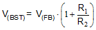
Equation 1. GUID-13B6AAED-276D-4AC6-A9E2-D592D2CF2013-low.gif

where

  • V(FB) = 1.32 V

V(BST) must be programmed to a value of 5.0 V greater than the largest peak voltage expected in the system to allow adequate amplifier headroom. Because the programming range for the boost voltage extends to 105 V, the leakage current through the resistor divider can become significant. It is recommended that the sum of the resistances R1 + R2 be greater than 400 kΩ. When resistor values greater than 1 MΩ are used, PCB contamination may cause boost voltage inaccuracy. Exercise caution when soldering large resistances, and clean the area when finished for best results. Table 7-2 shows examples on how to configure the device for different output voltages.

Table 7-2 Boost Voltage Table
R1R2GAIN[1:0]V(BST)FULL SCALE PEAK VOLTAGE (V)
402 kΩ18.2 kΩ003025
392 kΩ9.76 kΩ015550
768 kΩ13 kΩ108075
768 kΩ9.76 kΩ11105100