SLASF54 January 2023 DRV2901
PRODUCTION DATA
- 1 Features
- 2 Applications
- 3 Description
- 4 Revision History
- 5 Pin Configuration and Functions
- 6 Specifications
- 7 Detailed Description
- 8 Applications and Implementation
- 9 Power Supply Recommendations
- 10Mechanical, Packaging, and Orderable Information
Package Options
Mechanical Data (Package|Pins)
- DDV|44
Thermal pad, mechanical data (Package|Pins)
- DDV|44
Orderable Information
3 Description
The DRV2901 is a high performance lens cleaner transducer driver. This system only requires a simple passive LC demodulation filter to deliver high-quality, high-efficiency amplification with proven EMI compliance. This device requires two power supplies, at 12 V for GVDD and VDD, and 12 V to 48 V for PVDD. The DRV2901 does not require power-up sequencing due to internal power-on reset.
The DRV2901 has an innovative protection system integrated on-chip, safeguarding the device against a wide range of fault conditions that could damage the system. These safeguards are short-circuit protection, overcurrent protection, undervoltage protection, and overtemperature protection. The DRV2901 has a new proprietary current-limiting circuit that reduces the possibility of device shutdown during high-level transients.
| PART NUMBER | PACKAGE | BODY SIZE (NOM) |
|---|---|---|
| DRV2901 | 44-pin HTSSOP | 14.0 mm × 6.1 mm |
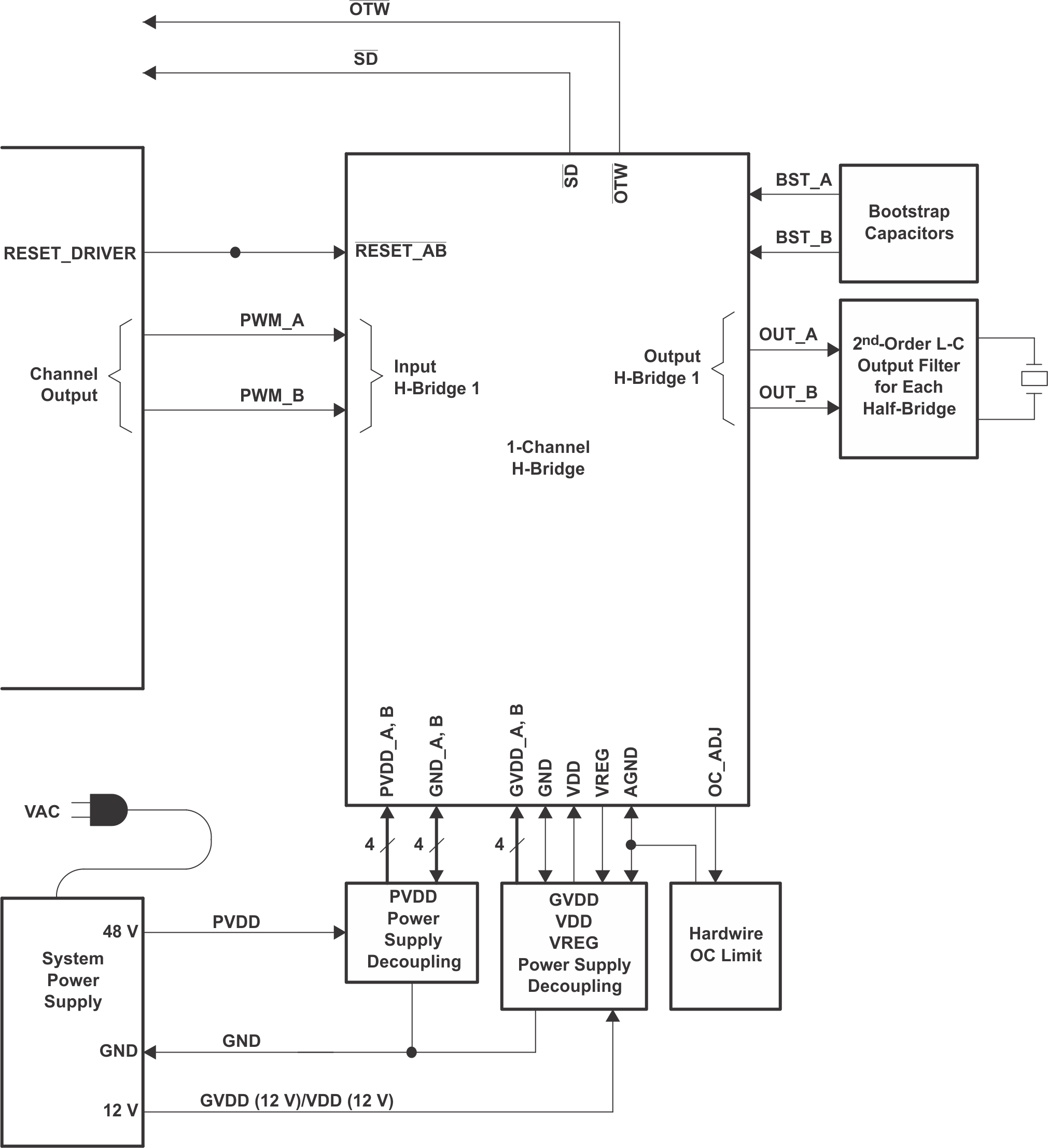
 DRV2901 Functional Block Diagram