SLVSG22B January 2023 – March 2024 DRV8145-Q1
PRODUCTION DATA
- 1
- 1 Features
- 2 Applications
- 3 Description
- 4 Device Comparison
- 5 Pin Configuration and Functions
-
6 Specifications
- 6.1 Absolute Maximum Ratings
- 6.2 ESD Ratings
- 6.3 Recommended Operating Conditions
- 6.4 Thermal Information
- 6.5
Electrical Characteristics
- 6.5.1 Power Supply & Initialization
- 6.5.2 Logic I/Os
- 6.5.3 SPI I/Os
- 6.5.4 Configuration Pins - HW Variant Only
- 6.5.5 Power FET Parameters
- 6.5.6 Switching Parameters with High-Side Recirculation
- 6.5.7 Switching Parameters with Low-Side Recirculation
- 6.5.8 IPROPI & ITRIP Regulation
- 6.5.9 Over Current Protection (OCP)
- 6.5.10 Over Temperature Protection (TSD)
- 6.5.11 Voltage Monitoring
- 6.5.12 Load Monitoring
- 6.5.13 Fault Retry Setting
- 6.5.14 Transient Thermal Impedance & Current Capability
- 6.6 SPI Timing Requirements
- 6.7 Switching Waveforms
- 6.8 Typical Characteristics
-
7 Detailed Description
- 7.1 Overview
- 7.2 Functional Block Diagram
- 7.3
Feature Description
- 7.3.1 External Components
- 7.3.2 Bridge Control
- 7.3.3 Device Configuration
- 7.3.4
Protection and Diagnostics
- 7.3.4.1 Over Current Protection (OCP)
- 7.3.4.2 Over Temperature Protection (TSD)
- 7.3.4.3 Off-State Diagnostics (OLP)
- 7.3.4.4 On-State Diagnostics (OLA) - SPI Variant Only
- 7.3.4.5 VM Over Voltage Monitor
- 7.3.4.6 VM Under Voltage Monitor
- 7.3.4.7 Charge pump under voltage monitor
- 7.3.4.8 Power On Reset (POR)
- 7.3.4.9 Event Priority
- 7.4 Programming - SPI Variant Only
- 8 Register Map - SPI Variant Only
- 9 Application and Implementation
- 10Device and Documentation Support
- 11Revision History
- 12Mechanical, Packaging, and Orderable Information
Package Options
Mechanical Data (Package|Pins)
Thermal pad, mechanical data (Package|Pins)
- PWP|28
Orderable Information
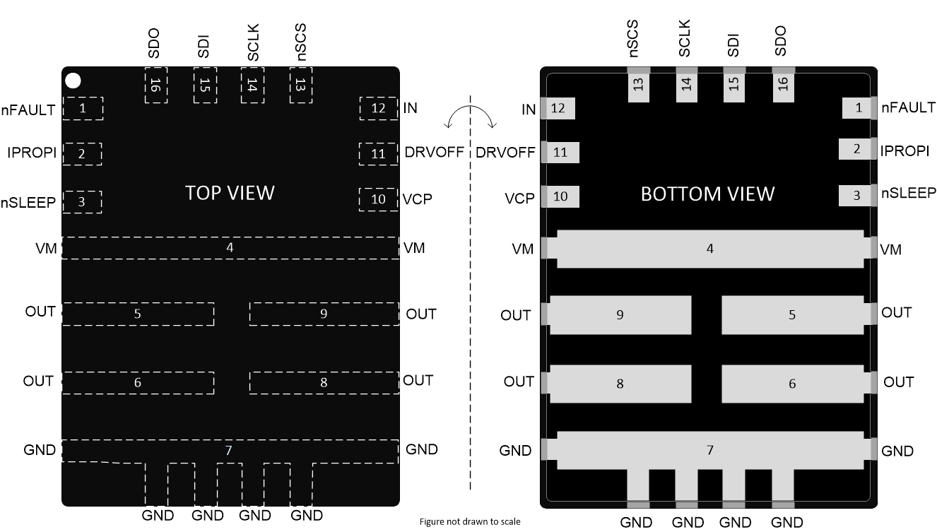
5.2.2 VQFN-HR(16) package
 Figure 5-3 DRV8145S-Q1 SPI(S) variant in VQFN-HR(16) package
Table 5-3 Pin Functions
| PIN | TYPE (1) | DESCRIPTION | |
|---|---|---|---|
| NO. | NAME | ||
| 1 | nFAULT | OD | Fault indication to the controller. For details, refer to nFAULT in the Device Configuration section. |
| 2 | IPROPI | I/O | Driver load current analog feedback. For details, refer to IPROPI in the Device Configuration section. |
| 3 | nSLEEP | I | Controller input pin for SLEEP. For details, see the Bridge Control section. Also VIO logic level for SDO. |
| 4 | VM | P | Power supply. This pin is the motor supply voltage. Bypass this pin to GND with a 0.1-µF ceramic capacitor and a bulk capacitor. |
| 5, 6, 8, 9 | OUT | P | Half-bridge output. Connect this pin to the motor or load. Must combine with the other OUT pins (4 total) to support device current capability. |
| 7 | GND | G | Ground pin |
| 10 | VCP | P | Charge Pump pin for storage cap. Connect a 6.3V, 1µF capacitor to VM supply. |
| 11 | DRVOFF | I | Controller input pin for bridge Hi-Z. For details, see the Bridge Control section. |
| 12 | IN | I | Controller input pin for bridge operation. For details, see the Bridge Control section. |
| 13 | nSCS | I | SPI - Chip Select. An active low on this pin enables the serial interface communication. |
| 14 | SCLK | I | SPI - Serial Clock input. |
| 15 | SDI | I | SPI - Serial Data Input. Data is captured at the falling edge of SCLK. |
| 16 | SDO | PP | SPI - Serial Data Output. Data is updated at the rising edge of SCLK. |
(1) I = input, O = output, I/O = input/output, G = ground, P = power,
OD = open-drain output, PP = push-pull output