SLVSFY8B February 2020 – August 2021 DRV8210
PRODUCTION DATA
- 1 Features
- 2 Applications
- 3 Description
- 4 Revision History
- 5 Device Comparison
- 6 Pin Configuration and Functions
- 7 Specifications
- 8 Detailed Description
- 9 Application and Implementation
- 10Power Supply Recommendations
- 11Layout
- 12Device and Documentation Support
- 13Mechanical, Packaging, and Orderable Information
Package Options
Mechanical Data (Package|Pins)
Thermal pad, mechanical data (Package|Pins)
- DSG|8
Orderable Information
9.2.2.2.3 Low-Power Operation
Bringing VCC to 0 V puts the DRV8210 to sleep in half-bridge mode. Section 8.4.2 describes how to enter low-power sleep mode in detail. When entering sleep mode, TI recommends setting all inputs as a logic low to minimize system power. To wake up the DRV8210 in half-bridge mode, bring VCC high, then set IN1 or IN2 high for longer than tWAKE before returning low or sending a PWM signal. Figure 9-19 and Figure 9-20 show this wakeup procedure.
Because of the decoupling capacitor on the VCC pin, TI recommends adding a resistor between the GPIO pin of the controller and the VCC pin as shown in Figure 9-9, Figure 9-10, and Figure 9-11. The purpose of this resistor is to protect the GPIO pin from large currents from the capacitor when switching the GPIO pin. However, this resistor must be sized appropriately to allow the operating current, IVCC, to flow into the VCC pin. Table 9-3 shows the design considerations for the RLIMIT resistor. VOL is the GPIO voltage when logic low, VOH is the GPIO voltage when logic high, and IOL is the maximum current that the GPIO can sink. The controller datasheet should specify VOL, VOH and IOL for the GPIO pin.
| Design consideration | Equation | Example |
|---|---|---|
| Minimum resistance needed to protect GPIO pin. Here, VCap is the voltage on the capacitor when the GPIO pin switches from high to low. To simplify calculation and assume a worst-case condition, VCap is assumed to be equivalent to the controller supply voltage, VMCU. See Figure 9-12 for example circuit. | RLimit ≥ (VCap - VOL) / IOL | RLimit ≥ (3.3 V - 0.3 V) / 24 mA = 125 Ω |
| Keep the VCC pin voltage high enough so device does not go into undervoltage lockout. See Figure 9-13 for example circuit. | VOH - (IVCC × RLimit) = VVCC ≥ 1.65 V | 3.0 V - (3.6 mA × 125 Ω) = 2.55 V ≥ 1.65 V |
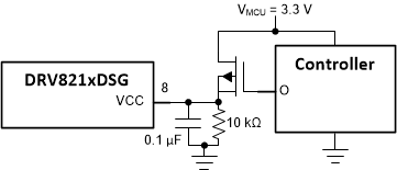
In cases where the specified GPIO current is too small, there are a few other options to put the device to sleep. One option is to parallel multiple GPIO to supply the appropriate current. A second option is to set MODE = IN1 = IN2 = 0 to put the device into the autosleep state. This will require the GPIO pin that controls MODE to be configured as an input during operation and an output low during sleep. A third option is to place a GPIO-controlled transistor between the supply and the VCC pin as shown in Figure 9-14.
 Figure 9-14 GPIO with transistor
To minimize leakage current into the OUTx pins (especially in battery-powered applications), connect the load from OUTx to GND. As mentioned earlier, connecting the load from OUTx to VM is also possible, but there may be some small leakage current into OUTx when it is disabled. No leakage current is expected if loads are connected in H-bridge configuration.