SLVSD12D May 2015 – July 2019 DRV8305-Q1
PRODUCTION DATA.
- 1 Features
- 2 Applications
- 3 Description
- 4 Revision History
- 5 Pin Configuration and Functions
- 6 Specifications
-
7 Detailed Description
- 7.1 Overview
- 7.2 Functional Block Diagram
- 7.3
Feature Description
- 7.3.1 Integrated Three-Phase Gate Driver
- 7.3.2 INHx/INLx: Gate Driver Input Modes
- 7.3.3 VCPH Charge Pump: High-Side Gate Supply
- 7.3.4 VCP_LSD LDO: Low-Side Gate Supply
- 7.3.5 GHx/GLx: Half-Bridge Gate Drivers
- 7.3.6 DVDD and AVDD: Internal Voltage Regulators
- 7.3.7 VREG: Voltage Regulator Output
- 7.3.8 Protection Features
- 7.3.9 Undervoltage Warning (UVFL), Undervoltage Lockout (UVLO), and Overvoltage (OV) Protection
- 7.4 Device Functional Modes
- 7.5 Programming
- 7.6
Register Maps
- 7.6.1 Status Registers
- 7.6.2
Control Registers
- 7.6.2.1 HS Gate Drive Control (Address = 0x5)
- 7.6.2.2 LS Gate Drive Control (Address = 0x6)
- 7.6.2.3 Gate Drive Control (Address = 0x7)
- 7.6.2.4 IC Operation (Address = 0x9)
- 7.6.2.5 Shunt Amplifier Control (Address = 0xA)
- 7.6.2.6 Voltage Regulator Control (Address = 0xB)
- 7.6.2.7 VDS Sense Control (Address = 0xC)
- 8 Application and Implementation
- 9 Power Supply Recommendations
- 10Layout
- 11Device and Documentation Support
- 12Mechanical, Packaging, and Orderable Information
Package Options
Mechanical Data (Package|Pins)
- PHP|48
Thermal pad, mechanical data (Package|Pins)
- PHP|48
Orderable Information
7.3.8.3 MOSFET Overcurrent Protection (VDS_OCP)
To protect the system and external MOSFET from damage due to high current events, VDS overcurrent monitors are implemented in the DRV8305-Q1.
The VDS sensing is implemented for both the high-side and low-side MOSFETs through the pins below:
- High-side MOSFET: VDS measured between VDRAIN and SHx pins.
- Low-side MOSFET: VDS measured between SHx and SLx pins.
Based on the RDS(on) of the power MOSFETs and the maximum allowed IDS, a voltage threshold can be calculated, which when exceeded, triggers the VDS overcurrent protection feature. The voltage threshold level (VDS_LEVEL) is programmable through the SPI VDS_LEVEL setting in register 0xC, bits D7-D3 and may be changed during gate driver operation if needed.
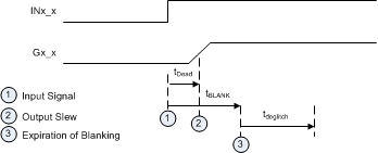
The VDS overcurrent monitors implement adjustable blanking and deglitch times to prevent false trips due to switching voltage transients. The VDS blanking time (tBLANK) is inserted digitally and programmable through the SPI TBLANK setting in register 0x7, bits D3-D2. The tBLANK time is inserted after each switch ON transistion (LOW to HIGH) of the output gate drivers is commanded. During the tBLANK time, the VDS comparators are not being monitored in order to prevent false trips when the MOSFET first turns ON. After the tBLANK time expires the overcurrent monitors will begin actively watching for an overcurrent event.
The VDS deglitch time (tVDS) is inserted digitally and programmable through the SPI TVDS setting in register 0x7, bits D1-D0. The tVDS time is a delay inserted after the VDS sensing comparators have tripped to when the protection logic is informed that a VDS event has occurred. If the overcurrent event does not persist through tVDS delay then it will be ignored by the DRV8305-Q1.
Note that the dead time and blanking time are overlapping timers as shown in Figure 13.
 Figure 13. VDS Deglitch and Blank Diagram
 The DRV8305-Q1 has three possible responses to a VDS overcurrent event. This response is set through the SPI VDS_MODE setting in register 0xC, bits D2-D0.
- VDS Latched Shutdown Mode:
- VDS Report Only Mode:
- VDS Disabled Mode:
When a VDS overcurrent event occurs, the device will pull all gate drive outputs low in order to put all six external MOSFETs into high impedance mode. The fault will be reported on the nFAULT pin with the specific MOSFET in which the overcurrent event was detected in reported through the SPI status registers.
In this mode, the device will take no action related to the gate drivers. When the overcurrent event is detected the fault will be reported on the nFAULT pin with the specific MOSFET in which the overcurrent event was detected in reported through the SPI status registers. The gate drivers will continue to operate normally.
The device ignores all the VDS overcurrent event detections and does not report them.