SLVSE38A April 2018 – July 2018 DRV8306
PRODUCTION DATA.
- 1 Features
- 2 Applications
- 3 Description
- 4 Revision History
- 5 Pin Configuration and Functions
- 6 Specifications
-
7 Detailed Description
- 7.1 Overview
- 7.2 Functional Block Diagram
- 7.3
Feature Description
- 7.3.1 Three Phase Smart Gate Drivers
- 7.3.2 DVDD Linear Voltage Regulator
- 7.3.3 Pulse-by-Pulse Current Limit
- 7.3.4 Hall Comparators
- 7.3.5 FGOUT Signal
- 7.3.6 Pin Diagrams
- 7.3.7 Gate-Driver Protective Circuits
- 7.4 Device Functional Modes
- 8 Application and Implementation
- 9 Power Supply Recommendations
- 10Layout
- 11Device and Documentation Support
- 12Mechanical, Packaging, and Orderable Information
Package Options
Mechanical Data (Package|Pins)
- RSM|32
Thermal pad, mechanical data (Package|Pins)
- RSM|32
Orderable Information
7.3.1.4.2 TDRIVE: MOSFET Gate Drive Control
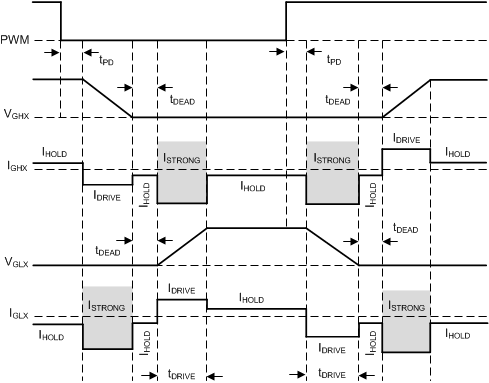
The TDRIVE component is an integrated gate-drive state machine that provides automatic dead time insertion through switching handshaking, parasitic dV/dt gate turnon prevention, and MOSFET gate-fault detection.
The first component of the TDRIVE state machine is automatic dead-time insertion. Dead time is period of time between the switching of the external high-side and low-side MOSFETs to ensure that they do not cross conduct and cause shoot-through. The DRV8306 device uses VGS voltage monitors to measure the MOSFET gate-to-source voltage and determine the proper time to switch instead of relying on a fixed time value. This feature allows the gate-driver dead time to adjust for variation in the system such as temperature drift and variation in the MOSFET parameters. An additional digital dead time (tDEAD) is inserted on top of the gate-driver dead time and is fixed for the DRV8306 device.
The second component focuses on prevention of parasitic dV/dt gate turnon. To implement this feature, the TDRIVE state machine enables a strong pulldown current (ISTRONG) on the opposite MOSFET gate whenever a MOSFET is switching. The strong pulldown last for the TDRIVE duration. This feature helps remove parasitic charge that couples into the MOSFET gate when the half-bridge switch-node voltage slews rapidly.
The third component implements a gate-fault detection scheme to detect pin-to-pin solder defects, a MOSFET gate failure, or a MOSFET gate stuck-high or stuck-low voltage condition. This implementation is done with a pair of VGS gate-to-source voltage monitors for each half-bridge gate driver. When the gate driver receives a command to change the state of the half-bridge it begins to monitor the gate voltage of the external MOSFET. If the VGS voltage has not reached the proper threshold at the end of the tDRIVE period, the gate driver reports a fault. To ensure that a false fault is not detected, the user must ensure that the tDRIVE time is longer than the time required to charge or discharge the MOSFET gate (this setting can be configured indirectly using the IDRIVE pin). The tDRIVE time does not increase the PWM time and will terminate if another PWM command is received while active. Additional details on the TDRIVE settings are described in the Pin Diagrams section for hardware interface devices.
Figure 13 shows an example of the TDRIVE state machine in operation.
 Figure 13. TDRIVE State Machine