SLVSFV1B August 2018 – August 2021 DRV8350F , DRV8353F
PRODUCTION DATA
- 1 Features
- 2 Applications
- 3 Description
- 4 Revision History
- 5 Device Comparison Table
- 6 Pin Configuration and Functions
- 7 Specifications
-
8 Detailed Description
- 8.1 Overview
- 8.2 Functional Block Diagram
- 8.3
Feature Description
- 8.3.1 Three Phase Smart Gate Drivers
- 8.3.2 DVDD Linear Voltage Regulator
- 8.3.3 Pin Diagrams
- 8.3.4 Low-Side Current-Shunt Amplifiers (DRV8353F)
- 8.3.5
Gate Driver Protective Circuits
- 8.3.5.1 VM Supply and VDRAIN Undervoltage Lockout (UVLO)
- 8.3.5.2 VCP Charge-Pump and VGLS Regulator Undervoltage Lockout (GDUV)
- 8.3.5.3 MOSFET VDS Overcurrent Protection (VDS_OCP)
- 8.3.5.4 VSENSE Overcurrent Protection (SEN_OCP)
- 8.3.5.5 Gate Driver Fault (GDF)
- 8.3.5.6 Overcurrent Soft Shutdown (OCP Soft)
- 8.3.5.7 Thermal Warning (OTW)
- 8.3.5.8 Thermal Shutdown (OTSD)
- 8.3.5.9 Fault Response Table
- 8.4 Device Functional Modes
- 8.5 Programming
- 8.6
Register Maps
- 8.6.1 Status Registers
- 8.6.2
Control Registers
- 8.6.2.1 Driver Control Register (address = 0x02h)
- 8.6.2.2 Gate Drive HS Register (address = 0x03h)
- 8.6.2.3 Gate Drive LS Register (address = 0x04h)
- 8.6.2.4 OCP Control Register (address = 0x05h)
- 8.6.2.5 CSA Control Register (DRV8353FOnly) (address = 0x06h)
- 8.6.2.6 Driver Configuration Register (DRV8353F Only) (address = 0x07h)
-
9 Application and Implementation
- 9.1 Application Information
- 9.2
Typical Application
- 9.2.1
Primary Application
- 9.2.1.1 Design Requirements
- 9.2.1.2 Detailed Design Procedure
- 9.2.1.3 Application Curves
- 9.2.2 Alternative Application
- 9.2.1
Primary Application
- 10Power Supply Recommendations
- 11Layout
- 12Device and Documentation Support
- 13Mechanical, Packaging, and Orderable Information
Package Options
Mechanical Data (Package|Pins)
- RTV|32
Thermal pad, mechanical data (Package|Pins)
- RTV|32
Orderable Information
8.3.1.1.3 1x PWM Mode (PWM_MODE = 10b or MODE Pin = Hi-Z)
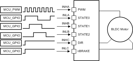
In this mode, the DRV835xF family of devices uses 6-step block commutation tables that are stored internally. This feature allows for a three-phase BLDC motor to be controlled using a single PWM sourced from a simple controller. The PWM is applied on the INHA pin and determines the output frequency and duty cycle of the half-bridges.
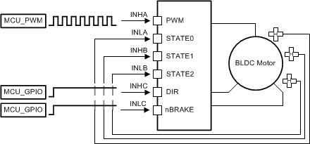
The half-bridge output states are managed by the INLA, INHB, and INLB pins which are used as state logic inputs. The state inputs can be controlled by an external controller or connected directly to hall sensor digital outputs from the motor (INLA = HALL_A, INHB = HALL_B, INLB = HALL_C). The 1x PWM mode usually operates with synchronous rectification, however it can be configured to use asynchronous diode freewheeling rectification on SPI devices. This configuration is set using the 1PWM_COM bit through the SPI registers.
The INHC input controls the direction through the 6-step commutation table which is used to change the direction of the motor when hall sensors are directly controlling the INLA, INHB, and INLB state inputs. Tie the INHC pin low if this feature is not required.
The INLC input brakes the motor by turning off all high-side MOSFETs and turning on all low-side MOSFETs when it is pulled low. This brake is independent of the states of the other input pins. Tie the INLC pin high if this feature is not required.
| LOGIC AND HALL INPUTS | GATE-DRIVE OUTPUTS | ||||||||||||
|---|---|---|---|---|---|---|---|---|---|---|---|---|---|
| STATE | INHC = 0 | INHC = 1 | PHASE A | PHASE B | PHASE C | DESCRIPTION | |||||||
| INLA | INHB | INLB | INLA | INHB | INLB | GHA | GLA | GHB | GLB | GHC | GLC | ||
| Stop | 0 | 0 | 0 | 0 | 0 | 0 | L | L | L | L | L | L | Stop |
| Align | 1 | 1 | 1 | 1 | 1 | 1 | PWM | !PWM | L | H | L | H | Align |
| 1 | 1 | 1 | 0 | 0 | 0 | 1 | L | L | PWM | !PWM | L | H | B → C |
| 2 | 1 | 0 | 0 | 0 | 1 | 1 | PWM | !PWM | L | L | L | H | A → C |
| 3 | 1 | 0 | 1 | 0 | 1 | 0 | PWM | !PWM | L | H | L | L | A → B |
| 4 | 0 | 0 | 1 | 1 | 1 | 0 | L | L | L | H | PWM | !PWM | C → B |
| 5 | 0 | 1 | 1 | 1 | 0 | 0 | L | H | L | L | PWM | !PWM | C → A |
| 6 | 0 | 1 | 0 | 1 | 0 | 1 | L | H | PWM | !PWM | L | L | B → A |
| LOGIC AND HALL INPUTS | GATE-DRIVE OUTPUTS | ||||||||||||
|---|---|---|---|---|---|---|---|---|---|---|---|---|---|
| STATE | INHC = 0 | INHC = 1 | PHASE A | PHASE B | PHASE C | DESCRIPTION | |||||||
| INLA | INHB | INLB | INLA | INHB | INLB | GHA | GLA | GHB | GLB | GHC | GLC | ||
| Stop | 0 | 0 | 0 | 0 | 0 | 0 | L | L | L | L | L | L | Stop |
| Align | 1 | 1 | 1 | 1 | 1 | 1 | PWM | L | L | H | L | H | Align |
| 1 | 1 | 1 | 0 | 0 | 0 | 1 | L | L | PWM | L | L | H | B → C |
| 2 | 1 | 0 | 0 | 0 | 1 | 1 | PWM | L | L | L | L | H | A → C |
| 3 | 1 | 0 | 1 | 0 | 1 | 0 | PWM | L | L | H | L | L | A → B |
| 4 | 0 | 0 | 1 | 1 | 1 | 0 | L | L | L | H | PWM | L | C → B |
| 5 | 0 | 1 | 1 | 1 | 0 | 0 | L | H | L | L | PWM | L | C → A |
| 6 | 0 | 1 | 0 | 1 | 0 | 1 | L | H | PWM | L | L | L | B → A |
Figure 8-5 and Figure 8-6 show the different possible configurations in 1x PWM mode.
 Figure 8-5 1x PWM—Simple Controller
 Figure 8-6 1x PWM—Hall Sensor