SLES242G December   2009  – December 2014 DRV8412

PRODUCTION DATA.  

  1. Features
  2. Applications
  3. Description
    1.     Simplified Application Diagram
  4. Revision History
  5. Pin Configuration and Functions
    1.     Pin Functions
  6. Specifications
    1. 6.1 Absolute Maximum Ratings
    2. 6.2 ESD Ratings
    3. 6.3 Recommended Operating Conditions
    4. 6.4 Thermal Information
    5. 6.5 Package Heat Dissipation Ratings
    6. 6.6 Package Power Deratings (DRV8412)
    7. 6.7 Electrical Characteristics
    8. 6.8 Typical Characteristics
  7. Detailed Description
    1. 7.1 Overview
    2. 7.2 Functional Block Diagram
    3. 7.3 Feature Description
      1. 7.3.1 Error Reporting
      2. 7.3.2 Device Protection System
        1. 7.3.2.1 Bootstrap Capacitor Undervoltage Protection
        2. 7.3.2.2 Overcurrent (OC) Protection
        3. 7.3.2.3 Overtemperature Protection
        4. 7.3.2.4 Undervoltage Protection (UVP) and Power-On Reset (POR)
      3. 7.3.3 Device Reset
    4. 7.4 Device Functional Modes
  8. Application and Implementation
    1. 8.1 Application Information
    2. 8.2 Typical Applications
      1. 8.2.1 Full Bridge Mode Operation
        1. 8.2.1.1 Design Requirements
        2. 8.2.1.2 Detailed Design Procedure
          1. 8.2.1.2.1 Motor Voltage
          2. 8.2.1.2.2 Current Requirement of 12-V Power Supply
          3. 8.2.1.2.3 Voltage of Decoupling Capacitor
          4. 8.2.1.2.4 Overcurrent Threshold
          5. 8.2.1.2.5 Sense Resistor
        3. 8.2.1.3 Application Curves
      2. 8.2.2 Parallel Full Bridge Mode Operation
      3. 8.2.3 Stepper Motor Operation
      4. 8.2.4 TEC Driver
      5. 8.2.5 LED Lighting Driver
  9. Power Supply Recommendations
    1. 9.1 Bulk Capacitance
    2. 9.2 Power Supplies
    3. 9.3 System Power-Up and Power-Down Sequence
      1. 9.3.1 Powering Up
      2. 9.3.2 Powering Down
    4. 9.4 System Design Recommendations
      1. 9.4.1 VREG Pin
      2. 9.4.2 VDD Pin
      3. 9.4.3 OTW Pin
      4. 9.4.4 Mode Select Pin
      5. 9.4.5 Parallel Mode Operation
      6. 9.4.6 TEC Driver Application
  10. 10Layout
    1. 10.1 Layout Guidelines
      1. 10.1.1 PCB Material Recommendation
      2. 10.1.2 Ground Plane
      3. 10.1.3 Decoupling Capacitor
      4. 10.1.4 AGND
    2. 10.2 Layout Example
      1. 10.2.1 Current Shunt Resistor
    3. 10.3 Thermal Considerations
      1. 10.3.1 DRV8412 Thermal Via Design Recommendation
  11. 11Device and Documentation Support
    1. 11.1 Related Links
    2. 11.2 Trademarks
    3. 11.3 Electrostatic Discharge Caution
    4. 11.4 Glossary
  12. 12Mechanical, Packaging, and Orderable Information

Package Options

Mechanical Data (Package|Pins)
Thermal pad, mechanical data (Package|Pins)
Orderable Information

Current Shunt Resistor

If current shunt resistor is connected between GND_X to GND or PVDD_X to PVDD, make sure there is only one single path to connect each GND_X or PVDD_X pin to shunt resistor, and the path is short and symmetrical on each sense path to minimize the measurement error due to additional resistance on the trace.

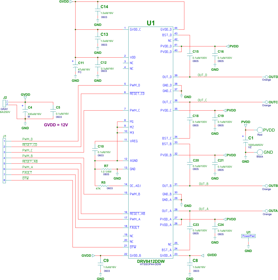
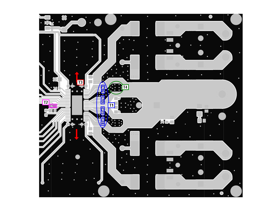
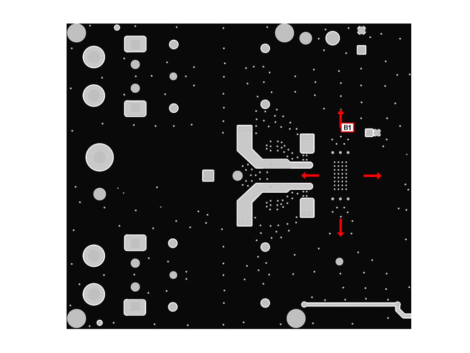
An example of the schematic and PCB layout of DRV8412 are shown in Figure 20, Figure 21, and Figure 22.
DRV8412 DRV8432 schem_pdf_8412_les242.gifFigure 20. DRV8412 Schematic Example
DRV8412 DRV8432 pcb-topA_les242.png
T1: PVDD decoupling capacitors C16, C19, C21, and C24 should be placed very close to PVDD_X pins and ground return path.
T2: VREG decoupling capacitor C10 should be placed very close to VREG abd AGND pins.
T3: Clear the space above and below the device as much as possible to improve the thermal spreading.
T4: Add many vias to reduce the impedance of ground path through top to bottom side. Make traces as wide as possible for ground path such as GND_X path.
Figure 21. Printed Circuit Board – Top Layer
DRV8412 DRV8432 pcb_bottomA_les242.png
B1: Do not block the heat transfer path at bottom side. Clear as much space as possible for better heat spreading.
Figure 22. Printed Circuit Board – Bottom Layer