SLES242G December   2009  – December 2014 DRV8412

PRODUCTION DATA.  

  1. Features
  2. Applications
  3. Description
    1.     Simplified Application Diagram
  4. Revision History
  5. Pin Configuration and Functions
    1.     Pin Functions
  6. Specifications
    1. 6.1 Absolute Maximum Ratings
    2. 6.2 ESD Ratings
    3. 6.3 Recommended Operating Conditions
    4. 6.4 Thermal Information
    5. 6.5 Package Heat Dissipation Ratings
    6. 6.6 Package Power Deratings (DRV8412)
    7. 6.7 Electrical Characteristics
    8. 6.8 Typical Characteristics
  7. Detailed Description
    1. 7.1 Overview
    2. 7.2 Functional Block Diagram
    3. 7.3 Feature Description
      1. 7.3.1 Error Reporting
      2. 7.3.2 Device Protection System
        1. 7.3.2.1 Bootstrap Capacitor Undervoltage Protection
        2. 7.3.2.2 Overcurrent (OC) Protection
        3. 7.3.2.3 Overtemperature Protection
        4. 7.3.2.4 Undervoltage Protection (UVP) and Power-On Reset (POR)
      3. 7.3.3 Device Reset
    4. 7.4 Device Functional Modes
  8. Application and Implementation
    1. 8.1 Application Information
    2. 8.2 Typical Applications
      1. 8.2.1 Full Bridge Mode Operation
        1. 8.2.1.1 Design Requirements
        2. 8.2.1.2 Detailed Design Procedure
          1. 8.2.1.2.1 Motor Voltage
          2. 8.2.1.2.2 Current Requirement of 12-V Power Supply
          3. 8.2.1.2.3 Voltage of Decoupling Capacitor
          4. 8.2.1.2.4 Overcurrent Threshold
          5. 8.2.1.2.5 Sense Resistor
        3. 8.2.1.3 Application Curves
      2. 8.2.2 Parallel Full Bridge Mode Operation
      3. 8.2.3 Stepper Motor Operation
      4. 8.2.4 TEC Driver
      5. 8.2.5 LED Lighting Driver
  9. Power Supply Recommendations
    1. 9.1 Bulk Capacitance
    2. 9.2 Power Supplies
    3. 9.3 System Power-Up and Power-Down Sequence
      1. 9.3.1 Powering Up
      2. 9.3.2 Powering Down
    4. 9.4 System Design Recommendations
      1. 9.4.1 VREG Pin
      2. 9.4.2 VDD Pin
      3. 9.4.3 OTW Pin
      4. 9.4.4 Mode Select Pin
      5. 9.4.5 Parallel Mode Operation
      6. 9.4.6 TEC Driver Application
  10. 10Layout
    1. 10.1 Layout Guidelines
      1. 10.1.1 PCB Material Recommendation
      2. 10.1.2 Ground Plane
      3. 10.1.3 Decoupling Capacitor
      4. 10.1.4 AGND
    2. 10.2 Layout Example
      1. 10.2.1 Current Shunt Resistor
    3. 10.3 Thermal Considerations
      1. 10.3.1 DRV8412 Thermal Via Design Recommendation
  11. 11Device and Documentation Support
    1. 11.1 Related Links
    2. 11.2 Trademarks
    3. 11.3 Electrostatic Discharge Caution
    4. 11.4 Glossary
  12. 12Mechanical, Packaging, and Orderable Information

Package Options

Mechanical Data (Package|Pins)
Thermal pad, mechanical data (Package|Pins)
Orderable Information

Typical Characteristics

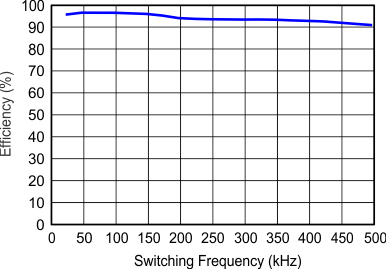
DRV8412 DRV8432 eff_freq_8ohm_les222.gif
Full Bridge Load = 5 A PVDD = 50 V Tc = 75°C
Figure 1. Efficiency vs Switching Frequency (DRV8432)
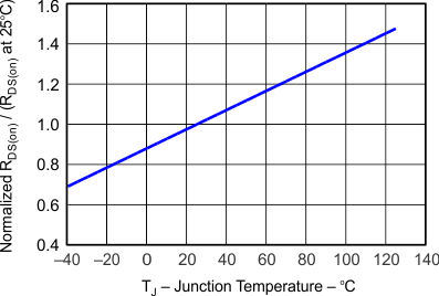
DRV8412 DRV8432 rds_v_gvdd12v_les222.gif
GVDD = 12 V
Figure 3. Normalized Rds(On) vs Junction Temperature
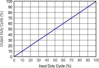
DRV8412 DRV8432 duty_cycle_les222.gif
fs = 500 kHz TC = 25°C
Figure 5. Output Duty Cycle vs Input Duty Cycle
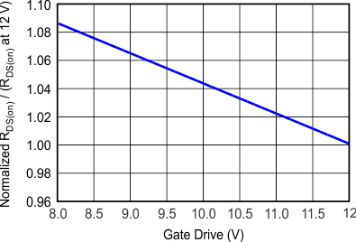
DRV8412 DRV8432 rds_v_gvdd_les222.gif
TJ = 25°C
Figure 2. Normalized RDS(On) vs Gate Drive
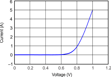
DRV8412 DRV8432 ds_diode_les222.gif
TJ = 25°C
Figure 4. Drain To Source Diode Forward On Characteristics