SLOSE60B May   2020  – May 2022 DRV8424E , DRV8425E

PRODUCTION DATA  

  1. Features
  2. Applications
  3. Description
  4. Revision History
  5. Pin Configuration and Functions
    1.     Pin Functions
  6. Specifications
    1. 6.1 Absolute Maximum Ratings
    2. 6.2 ESD Ratings
    3. 6.3 Recommended Operating Conditions
    4. 6.4 Thermal Information
    5. 6.5 Electrical Characteristics
    6. 6.6 Typical Characteristics
  7. Detailed Description
    1. 7.1 Overview
    2. 7.2 Functional Block Diagrams
    3. 7.3 Feature Description
      1. 7.3.1 PWM Motor Drivers
      2. 7.3.2 Bridge Control
      3. 7.3.3 Current Regulation
      4. 7.3.4 Decay Modes
        1. 7.3.4.1 Mixed Decay
        2. 7.3.4.2 Fast Decay
        3. 7.3.4.3 Smart tune Dynamic Decay
        4. 7.3.4.4 Smart tune Ripple Control
        5. 7.3.4.5 Blanking time
      5. 7.3.5 Charge Pump
      6. 7.3.6 Linear Voltage Regulators
      7. 7.3.7 Logic and Quad-Level Pin Diagrams
      8. 7.3.8 nFAULT Pin
      9. 7.3.9 Protection Circuits
        1. 7.3.9.1 VM Undervoltage Lockout (UVLO)
        2. 7.3.9.2 VCP Undervoltage Lockout (CPUV)
        3. 7.3.9.3 Overcurrent Protection (OCP)
        4. 7.3.9.4 Thermal Shutdown (OTSD)
        5. 7.3.9.5 Fault Condition Summary
    4. 7.4 Device Functional Modes
      1. 7.4.1 Sleep Mode (nSLEEP = 0)
      2. 7.4.2 Operating Mode (nSLEEP = 1)
      3. 7.4.3 nSLEEP Reset Pulse
      4. 7.4.4 Functional Modes Summary
  8. Application and Implementation
    1. 8.1 Application Information
    2. 8.2 Typical Application
      1. 8.2.1 Design Requirements
      2. 8.2.2 Detailed Design Procedure
        1. 8.2.2.1 Current Regulation
        2. 8.2.2.2 Power Dissipation and Thermal Calculation
      3. 8.2.3 Application Curves
    3. 8.3 Alternate Application
      1. 8.3.1 Design Requirements
      2. 8.3.2 Detailed Design Procedure
        1. 8.3.2.1 Current Regulation
        2. 8.3.2.2 Stepper Motor Speed
        3. 8.3.2.3 Decay Modes
  9. Power Supply Recommendations
    1. 9.1 Bulk Capacitance
  10. 10Layout
    1. 10.1 Layout Guidelines
    2. 10.2 Layout Example
  11. 11Device and Documentation Support
    1. 11.1 Documentation Support
      1. 11.1.1 Related Documentation
    2. 11.2 Related Links
    3. 11.3 Receiving Notification of Documentation Updates
    4. 11.4 Community Resources
    5. 11.5 Trademarks
  12. 12Mechanical, Packaging, and Orderable Information

Package Options

Mechanical Data (Package|Pins)
Thermal pad, mechanical data (Package|Pins)
Orderable Information

Feature Description

The following table shows the recommended values of the external components for the driver.
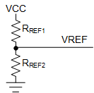
GUID-9D01D889-8E7E-4597-958C-E9DBC65E9FA8-low.gifFigure 7-3 Resistor divider connected to the VREF pins

Table 7-1 External Components
COMPONENTPIN 1PIN 2RECOMMENDED
CVM1VMPGNDTwo X7R, 0.01-µF, VM-rated ceramic capacitors
CVM2VMPGNDBulk, VM-rated capacitor
CVCPVCPVMX7R, 0.22-µF, 16-V ceramic capacitor
CSWCPHCPLX7R, 0.022-µF, VM-rated ceramic capacitor
CDVDDDVDDGNDX7R, 0.47-µF to 1-µF, 6.3-V or 10-V rated ceramic capacitor
RnFAULTVCC nFAULT>4.7-kΩ resistor
RREF1VREFxVCCResistor to limit chopping current. It is recommended that the value of parallel combination of RREF1 and RREF2 should be less than 50-kΩ.
RREF2 (Optional)VREFxGND