SLOSE49 November   2020 DRV8434E

PRODUCTION DATA  

  1. Features
  2. Applications
  3. Description
  4. Revision History
  5. Pin Configuration and Functions
    1.     Pin Functions
  6. Specifications
    1. 6.1 Absolute Maximum Ratings
    2. 6.2 ESD Ratings
    3. 6.3 Recommended Operating Conditions
    4. 6.4 Thermal Information
    5. 6.5 Electrical Characteristics
      1. 6.5.1 Typical Characteristics
  7. Detailed Description
    1. 7.1 Overview
    2. 7.2 Functional Block Diagrams
    3. 7.3 Feature Description
      1. 7.3.1 Bridge Control
      2. 7.3.2 Current Regulation
      3. 7.3.3 Decay Modes
        1. 7.3.3.1 Mixed Decay
        2. 7.3.3.2 Fast Decay
        3. 7.3.3.3 Smart tune Dynamic Decay
        4. 7.3.3.4 Smart tune Ripple Control
        5. 7.3.3.5 Blanking time
      4. 7.3.4 Charge Pump
      5. 7.3.5 Linear Voltage Regulators
      6. 7.3.6 Logic and Quad-Level Pin Diagrams
        1. 7.3.6.1 nFAULT Pin
      7. 7.3.7 Protection Circuits
        1. 7.3.7.1 VM Undervoltage Lockout (UVLO)
        2. 7.3.7.2 VCP Undervoltage Lockout (CPUV)
        3. 7.3.7.3 Overcurrent Protection (OCP)
        4. 7.3.7.4 Thermal Shutdown (OTSD)
        5.       Fault Condition Summary
    4. 7.4 Device Functional Modes
      1. 7.4.1 Sleep Mode (nSLEEP = 0)
      2. 7.4.2 Operating Mode (nSLEEP = 1)
      3. 7.4.3 nSLEEP Reset Pulse
      4.      Functional Modes Summary
  8. Application and Implementation
    1. 8.1 Application Information
    2. 8.2 Typical Application
      1. 8.2.1 Design Requirements
      2. 8.2.2 Detailed Design Procedure
        1. 8.2.2.1 Current Regulation
        2. 8.2.2.2 Power Dissipation and Thermal Calculation
      3. 8.2.3 Application Curves
    3. 8.3 Alternate Application
      1. 8.3.1 Design Requirements
      2. 8.3.2 Detailed Design Procedure
        1. 8.3.2.1 Current Regulation
        2. 8.3.2.2 Stepper Motor Speed
        3. 8.3.2.3 Decay Modes
  9. Power Supply Recommendations
    1. 9.1 Bulk Capacitance
  10. 10Layout
    1. 10.1 Layout Guidelines
    2. 10.2 Layout Example
  11. 11Mechanical, Packaging, and Orderable Information

Package Options

Mechanical Data (Package|Pins)
Thermal pad, mechanical data (Package|Pins)
Orderable Information

Application Curves

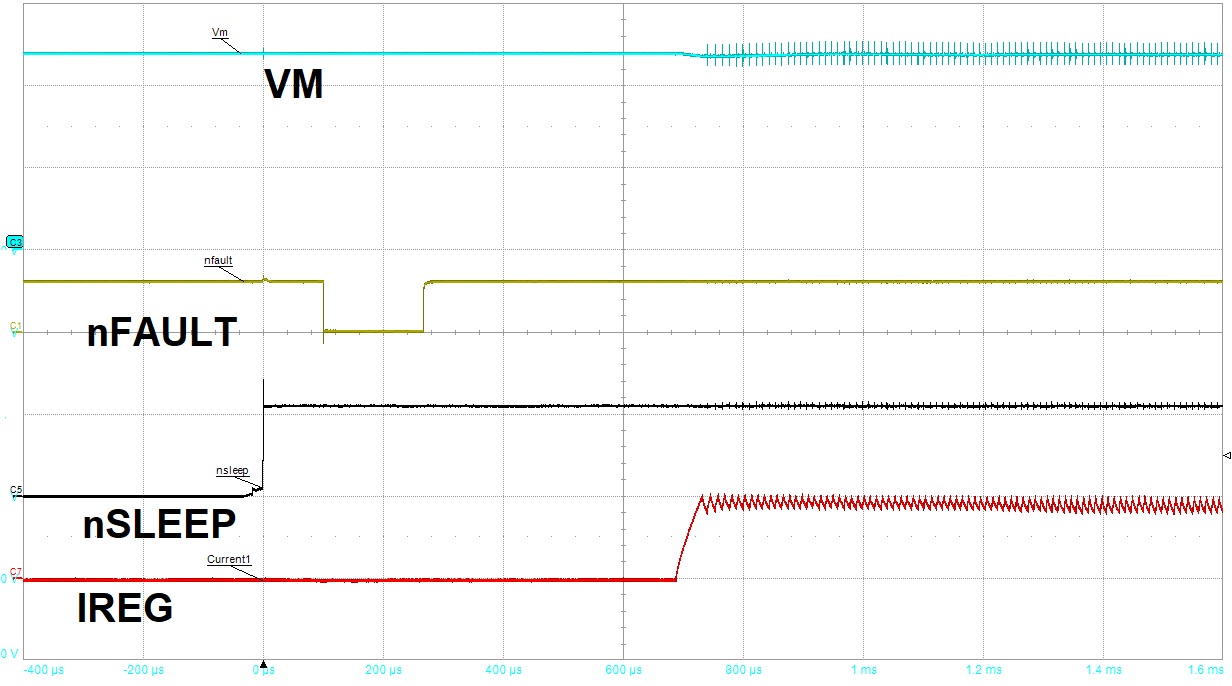
GUID-70CAFEE4-7801-49FD-B4B4-E47910A5C30E-low.jpgFigure 8-2 Device Power-up with nSLEEP. CH3 = VM (10V/div), CH1 = nFAULT (3V/div), CH5 = nSLEEP (3V/div), CH7 = IREG (1.5A/div)
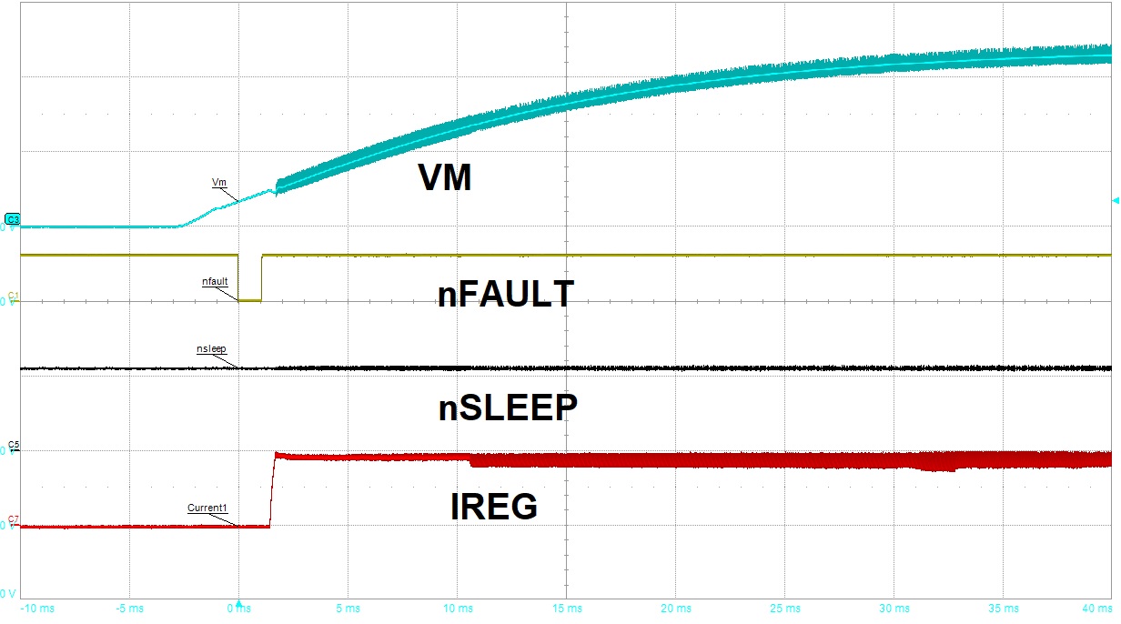
GUID-1F5D0E2B-F14F-4FFC-B30F-0C5F9E19B1E0-low.jpgFigure 8-3 Device Power-up with Supply Voltage (VM) Ramp. CH3 = VM (10V/div), CH1 = nFAULT (3V/div), CH5 = nSLEEP (3V/div), CH7 = IREG (1.5A/div)
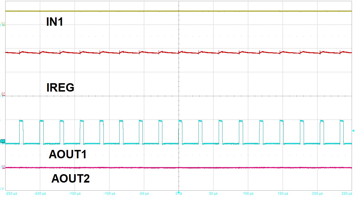
GUID-7BEBBCA2-7630-4F27-BCDC-1F73D27EB5D5-low.jpg Figure 8-4 Driver Full On Operation with Current Regulation. CH1 = IN1 (3V/div), CH7 = IREG (0.75A/div), CH3 = AOUT1 (24V/div), CH2 = AOUT2 (24V/div)