SLOSE49 November   2020 DRV8434E

PRODUCTION DATA  

  1. Features
  2. Applications
  3. Description
  4. Revision History
  5. Pin Configuration and Functions
    1.     Pin Functions
  6. Specifications
    1. 6.1 Absolute Maximum Ratings
    2. 6.2 ESD Ratings
    3. 6.3 Recommended Operating Conditions
    4. 6.4 Thermal Information
    5. 6.5 Electrical Characteristics
      1. 6.5.1 Typical Characteristics
  7. Detailed Description
    1. 7.1 Overview
    2. 7.2 Functional Block Diagrams
    3. 7.3 Feature Description
      1. 7.3.1 Bridge Control
      2. 7.3.2 Current Regulation
      3. 7.3.3 Decay Modes
        1. 7.3.3.1 Mixed Decay
        2. 7.3.3.2 Fast Decay
        3. 7.3.3.3 Smart tune Dynamic Decay
        4. 7.3.3.4 Smart tune Ripple Control
        5. 7.3.3.5 Blanking time
      4. 7.3.4 Charge Pump
      5. 7.3.5 Linear Voltage Regulators
      6. 7.3.6 Logic and Quad-Level Pin Diagrams
        1. 7.3.6.1 nFAULT Pin
      7. 7.3.7 Protection Circuits
        1. 7.3.7.1 VM Undervoltage Lockout (UVLO)
        2. 7.3.7.2 VCP Undervoltage Lockout (CPUV)
        3. 7.3.7.3 Overcurrent Protection (OCP)
        4. 7.3.7.4 Thermal Shutdown (OTSD)
        5.       Fault Condition Summary
    4. 7.4 Device Functional Modes
      1. 7.4.1 Sleep Mode (nSLEEP = 0)
      2. 7.4.2 Operating Mode (nSLEEP = 1)
      3. 7.4.3 nSLEEP Reset Pulse
      4.      Functional Modes Summary
  8. Application and Implementation
    1. 8.1 Application Information
    2. 8.2 Typical Application
      1. 8.2.1 Design Requirements
      2. 8.2.2 Detailed Design Procedure
        1. 8.2.2.1 Current Regulation
        2. 8.2.2.2 Power Dissipation and Thermal Calculation
      3. 8.2.3 Application Curves
    3. 8.3 Alternate Application
      1. 8.3.1 Design Requirements
      2. 8.3.2 Detailed Design Procedure
        1. 8.3.2.1 Current Regulation
        2. 8.3.2.2 Stepper Motor Speed
        3. 8.3.2.3 Decay Modes
  9. Power Supply Recommendations
    1. 9.1 Bulk Capacitance
  10. 10Layout
    1. 10.1 Layout Guidelines
    2. 10.2 Layout Example
  11. 11Mechanical, Packaging, and Orderable Information

Package Options

Mechanical Data (Package|Pins)
Thermal pad, mechanical data (Package|Pins)
Orderable Information

Feature Description

The following table shows the recommended values of the external components for the driver.
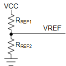
GUID-9D01D889-8E7E-4597-958C-E9DBC65E9FA8-low.gif Figure 7-3 Resistor divider connected to the VREF pins

Table 7-1 External Components
COMPONENT PIN 1 PIN 2 RECOMMENDED
CVM1 VM PGND Two X7R, 0.01-µF, VM-rated ceramic capacitors
CVM2 VM PGND Bulk, VM-rated capacitor
CVCP VCP VM X7R, 0.22-µF, 16-V ceramic capacitor
CSW CPH CPL X7R, 0.022-µF, VM-rated ceramic capacitor
CDVDD DVDD GND X7R, 0.47-µF to 1-µF, 6.3-V or 10-V rated ceramic capacitor
RnFAULT VCC nFAULT >4.7-kΩ resistor
RREF1 VREFx VCC Resistor to limit chopping current. It is recommended that the value of parallel combination of RREF1 and RREF2 should be less than 50-kΩ.
RREF2 (Optional) VREFx GND
VCC is not a pin on the device, but a VCC supply voltage pullup is required for open-drain output nFAULT; nFAULT may be pulled up to DVDD.