SLOSE37B June 2020 – May 2022 DRV8436
PRODUCTION DATA
- 1 Features
- 2 Applications
- 3 Description
- 4 Revision History
- 5 Pin Configuration and Functions
- 6 Specifications
-
7 Detailed Description
- 7.1 Overview
- 7.2 Functional Block Diagram
- 7.3
Feature Description
- 7.3.1 Stepper Motor Driver Current Ratings
- 7.3.2 PWM Motor Drivers
- 7.3.3 Microstepping Indexer
- 7.3.4 Controlling VREF with an MCU DAC
- 7.3.5 Current Regulation
- 7.3.6
Decay Modes
- 7.3.6.1 Slow Decay for Increasing and Decreasing Current
- 7.3.6.2 Slow Decay for Increasing Current, Mixed Decay for Decreasing Current
- 7.3.6.3 Mixed Decay for Increasing and Decreasing Current
- 7.3.6.4 Smart tune Dynamic Decay
- 7.3.6.5 Smart tune Ripple Control
- 7.3.6.6 PWM OFF Time
- 7.3.6.7 Blanking time
- 7.3.7 Charge Pump
- 7.3.8 Linear Voltage Regulators
- 7.3.9 Logic Level, tri-level and quad-level Pin Diagrams
- 7.3.10 Protection Circuits
- 7.4 Device Functional Modes
- 8 Application and Implementation
- 9 Thermal Application
- 10Layout
- 11Device and Documentation Support
- 12Mechanical, Packaging, and Orderable Information
Package Options
Mechanical Data (Package|Pins)
Thermal pad, mechanical data (Package|Pins)
- RGE|24
Orderable Information
7.3.5 Current Regulation
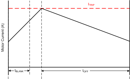
The current through the motor windings is regulated by an adjustable, off-time PWM current-regulation circuit. When an H-bridge is enabled, current rises through the winding at a rate dependent on the DC voltage, inductance of the winding, and the magnitude of the back EMF present. When the current hits the current regulation threshold, the bridge enters a decay mode for a period of time determined by the TOFF pin setting to decrease the current. After the off-time expires, the bridge is re-enabled, starting another PWM cycle.
 Figure 7-6 Current Chopping Waveform
The PWM regulation current is set by a comparator which monitors the voltage across the current sense MOSFETs in parallel with the low-side power MOSFETs. The current sense MOSFETs are biased with a reference current that is the output of a current-mode sine-weighted DAC whose full-scale reference current is set by the voltage at the VREF pin.
The full-scale regulation current (IFS) can be calculated as IFS (A) = VREF (V) / KV (V/A) = VREF (V) / 2.2 (V/A).