SLVSDR9E October 2016 – January 2021 DRV8702-Q1 , DRV8703-Q1
PRODUCTION DATA
- 1 Features
- 2 Applications
- 3 Description
- 4 Revision History
- 5 Pin Configuration and Functions
- 6 Specifications
-
7 Detailed Description
- 7.1 Overview
- 7.2 Functional Block Diagram
- 7.3
Feature Description
- 7.3.1 Bridge Control
- 7.3.2 MODE Pin
- 7.3.3 nFAULT Pin
- 7.3.4 Current Regulation
- 7.3.5 Amplifier Output (SO)
- 7.3.6 PWM Motor Gate Drivers
- 7.3.7 IDRIVE Pin (DRV8702-Q1 Only)
- 7.3.8 Dead Time
- 7.3.9 Propagation Delay
- 7.3.10 Overcurrent VDS Monitor
- 7.3.11 VDS Pin (DRV8702-Q1 Only)
- 7.3.12 Charge Pump
- 7.3.13 Gate Drive Clamp
- 7.3.14
Protection Circuits
- 7.3.14.1 VM Undervoltage Lockout (UVLO2)
- 7.3.14.2 Logic Undervoltage (UVLO1)
- 7.3.14.3 VCP Undervoltage Lockout (CPUV)
- 7.3.14.4 Overcurrent Protection (OCP)
- 7.3.14.5 Gate Driver Fault (GDF)
- 7.3.14.6 Thermal Shutdown (TSD)
- 7.3.14.7 Watchdog Fault (WDFLT, DRV8703-Q1 Only)
- 7.3.14.8 Reverse Supply Protection
- 7.3.15 Hardware Interface
- 7.4 Device Functional Modes
- 7.5 Programming
- 7.6 Register Maps
- 8 Application and Implementation
- 9 Power Supply Recommendations
- 10Layout
- 11Device and Documentation Support
- 12Mechanical, Packaging, and Orderable Information
Package Options
Refer to the PDF data sheet for device specific package drawings
Mechanical Data (Package|Pins)
- RHB|32
Thermal pad, mechanical data (Package|Pins)
Orderable Information
8.2.2.1 External FET Selection
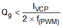
The DRV8702-Q1 FET support is based on the charge-pump capacity and PWM-output frequency. For a quick calculation of FET driving capacity, use Equation 3 when drive and brake (slow decay) are the primary modes of operation.

where
- fPWM is the maximum desired PWM frequency to be applied to the DRV8702-Q1 inputs or the current chopping frequency, whichever is larger.
- IVCP is the charge-pump capacity, which depends on the VM voltage.
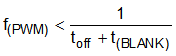
The internal current chopping frequency is at most equal to the PWM frequency as shown in Equation 4.
For example, if the VM voltage of a system is 7 V (IVCP = 8 mA) and uses a maximum PWM frequency of 40 kHz, then the DRV8702-Q1 device will support FETs with a Qg up to 200 nC.
If the application requires a forced fast decay (or alternating between drive and reverse drive), use Equation 5 to calculate the maximum FET driving capacity.