SLVSDX8B March   2017  – December 2018 DRV8702D-Q1 , DRV8703D-Q1

PRODUCTION DATA.  

  1. Features
  2. Applications
  3. Description
    1.     Device Images
      1.      Simplified Schematic
  4. Revision History
  5. Pin Configuration and Functions
    1.     Pin Functions
  6. Specifications
    1. 6.1 Absolute Maximum Ratings
    2. 6.2 ESD Ratings
    3. 6.3 Recommended Operating Conditions
    4. 6.4 Thermal Information
    5. 6.5 Electrical Characteristics
    6. 6.6 SPI Timing Requirements
    7. 6.7 Switching Characteristics
    8. 6.8 Typical Characteristics
  7. Detailed Description
    1. 7.1 Overview
    2. 7.2 Functional Block Diagram
    3. 7.3 Feature Description
      1. 7.3.1  Bridge Control
        1. 7.3.1.1 Logic Tables
      2. 7.3.2  MODE Pin
      3. 7.3.3  nFAULT Pin
      4. 7.3.4  Current Regulation
      5. 7.3.5  Amplifier Output (SO)
        1. 7.3.5.1 SO Sample and Hold Operation
      6. 7.3.6  PWM Motor Gate Drivers
        1. 7.3.6.1 Miller Charge (QGD)
      7. 7.3.7  IDRIVE Pin (DRV8702D-Q1 Only)
      8. 7.3.8  Dead Time
      9. 7.3.9  Propagation Delay
      10. 7.3.10 Overcurrent VDS Monitor
      11. 7.3.11 VDS Pin (DRV8702D-Q1 Only)
      12. 7.3.12 Charge Pump
      13. 7.3.13 Gate Drive Clamp
      14. 7.3.14 Protection Circuits
        1. 7.3.14.1 VM Undervoltage Lockout (UVLO2)
        2. 7.3.14.2 Logic Undervoltage (UVLO1)
        3. 7.3.14.3 VCP Undervoltage Lockout (CPUV)
        4. 7.3.14.4 Overcurrent Protection (OCP)
        5. 7.3.14.5 Gate Driver Fault (GDF)
        6. 7.3.14.6 Thermal Shutdown (TSD)
        7. 7.3.14.7 Watchdog Fault (WDFLT, DRV8703D-Q1 Only)
        8. 7.3.14.8 Reverse Supply Protection
      15. 7.3.15 Hardware Interface
        1. 7.3.15.1 IDRIVE (6-level input)
        2. 7.3.15.2 VDS (6-Level Input)
    4. 7.4 Device Functional Modes
    5. 7.5 Programming
      1. 7.5.1 SPI Communication
        1. 7.5.1.1 Serial Peripheral Interface (SPI)
        2. 7.5.1.2 SPI Format
    6. 7.6 Register Maps
      1. 7.6.1 DRV8703D-Q1 Memory Map
      2. 7.6.2 Status Registers
        1. 7.6.2.1 FAULT Status Register (address = 0x00h)
          1. Table 15. FAULT Status Field Descriptions
        2. 7.6.2.2 VDS and GDF Status Register Name (address = 0x01h)
          1. Table 16. VDS and GDF Status Field Descriptions
      3. 7.6.3 Control Registers
        1. 7.6.3.1 Main Control Register Name (address = 0x02h)
          1. Table 18. Main Control Field Descriptions
        2. 7.6.3.2 IDRIVE and WD Control Register Name (address = 0x03h)
          1. Table 19. IDRIVE and WD Field Descriptions
        3. 7.6.3.3 VDS Control Register Name (address = 0x04h)
          1. Table 21. VDS Control Field Descriptions
        4. 7.6.3.4 Config Control Register Name (address = 0x05h)
          1. Table 22. Config Control Field Descriptions
  8. Application and Implementation
    1. 8.1 Application Information
    2. 8.2 Typical Application
      1. 8.2.1 Design Requirements
      2. 8.2.2 Detailed Design Procedure
        1. 8.2.2.1 External FET Selection
        2. 8.2.2.2 IDRIVE Configuration
        3. 8.2.2.3 VDS Configuration
        4. 8.2.2.4 Current Chopping Configuration
      3. 8.2.3 Application Curves
  9. Power Supply Recommendations
    1. 9.1 Bulk Capacitance Sizing
  10. 10Layout
    1. 10.1 Layout Guidelines
    2. 10.2 Layout Example
  11. 11Device and Documentation Support
    1. 11.1 Documentation Support
      1. 11.1.1 Related Documentation
    2. 11.2 Related Links
    3. 11.3 Receiving Notification of Documentation Updates
    4. 11.4 Community Resources
    5. 11.5 Trademarks
    6. 11.6 Electrostatic Discharge Caution
    7. 11.7 Glossary
  12. 12Mechanical, Packaging, and Orderable Information

Package Options

Refer to the PDF data sheet for device specific package drawings

Mechanical Data (Package|Pins)
  • RHB|32
Thermal pad, mechanical data (Package|Pins)
Orderable Information

Bridge Control

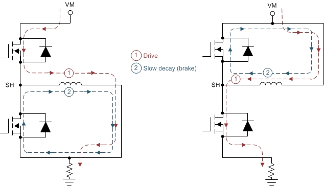
The DRV870xD-Q1 device is controlled using a configurable input interface. The Logic Tables section provides the half-bridge operation states. These tables do not consider the current control built into the DRV870xD-Q1 device. The logic operation set by the MODE pin is latched on power-up or when exiting sleep mode. Figure 31 shows the direction of the flow of current through the load when it is connected between the SH pin and GND, and between the SH pin and VM.
DRV8702D-Q1 DRV8703D-Q1 drv870xd-q1-bridge-control.gifFigure 31. Bridge Control